Optimizing High-Throughput SEM for Large-area Defect Characterization in AM Steel
Results and Discussion
Evaluation of Automated Detection Framework
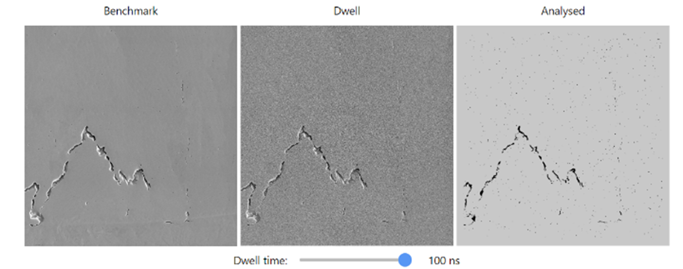
To initially assess the accuracy of our automated feature detection algorithm, we compared its results to manually labeled data subsets, with areas randomly selected across multiple dwell times. A constant pixel size of 195 nm per pixel was maintained throughout the analysis. Three annotators labeled 21 areas, each measuring 500x500 pixels, with areas randomly assigned among them. This random sampling captured a wide range of defects, minimizing both the effects of feature shape and potential biases from individual annotators. The results of this comparison are presented in Figure 3.1. On the left, the benchmark dataset is displayed, showing the investigated area of the sample. The middle panel illustrates the same area acquired at different dwell times, adjustable via the slider, enabling a comparison of image quality and defect visibility. On the right, the manually labeled areas (in red) are compared with those detected by the algorithm (in blue), with areas of agreement highlighted in green.
The two results were overlapped to evaluate the percent (%) of agreement between the algorithm’s detection and manual labels, and accuracy was expressed as the percentage of the pixel area in the algorithm detection that directly matched the manual labels. The agreement (%) is presented in Figure 3.2, with values averaged and standard deviations calculated across three tiles per dwell time.
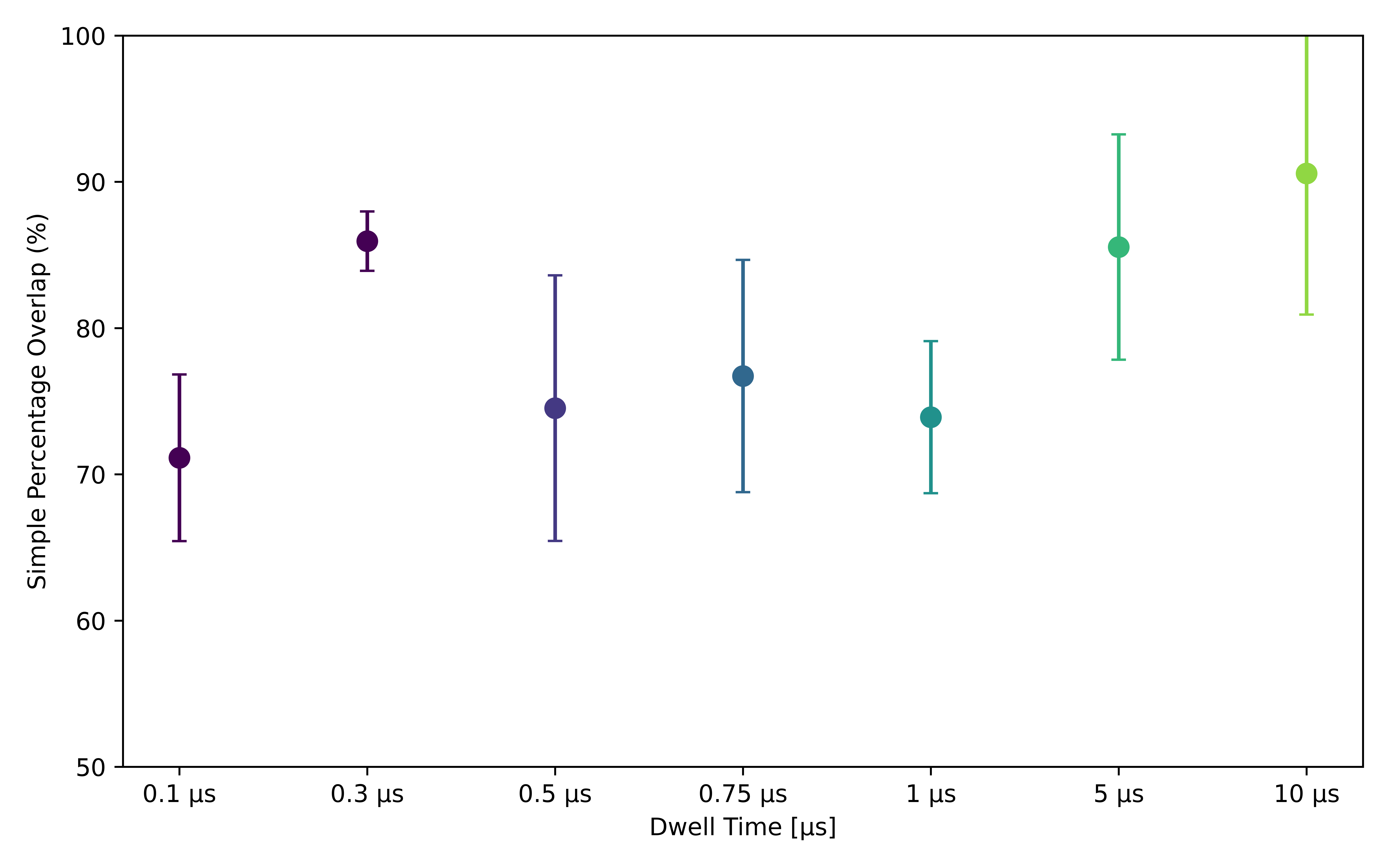
Figure 3.2:Calculated values of percentage overlap between algorithm results and manual labels
Figure 3.2 shows that even at the highest dwell time of 10 µs, only an agreement of 90 % was achieved between the manual labeling and the algorithm. This limited agreement underscores the very subjective nature of defining the exact boundaries of defects. The somewhat low agreement could result from edge effects in SE images or from smearing of defect edges during sample preparation, both of which can make it challenging to determine the exact border of a defect. This not only highlights the subjectivity involved in manual labeling but also the need for an automated detection algorithm.
However, the overall agreement between the manual labeling and the areas detected by the algorithm does not significantly decrease with a decrease in dwell time. For example, at the highest dwell time of 10 µs, the agreement is around 90 %; at an intermediate dwell time of 1 µs, it is 74 %; and even at the lowest dwell time of 100 ns, it remains at 72 %. This slight decline of approximately 16 % across a hundred times reduction in dwell time suggests that changes in dwell time have minimal impact on agreement, indicating the algorithm’s robustness.
Evaluation of SEM Acquisition Settings on Detection Accuracy
In the following sections, we will first evaluate the effects of pixel size and dwell time independently to understand their individual impacts on detection accuracy and consistency. In the final section, we will discuss the combined effects of these factors on overall high-throughput performance, considering the trade-offs involved in optimizing both detection accuracy and acquisition speed.
Effect of Pixel Size
Pixel size in SEM images is a crucial factor significantly impacting total image acquisition time while also defining the size of the smallest detectable feature. This section highlights how the choice of pixel size affects the defect detectability of our framework and influences the statistical evaluation of defects in our AM steel sample. All data presented in this section was acquired with a dwell time of 1 µs.
The presented algorithm analyzes local image contrast on a pixel basis. A minimum defect size constraint is applied to ensure cohesive defect identification and reduce the detection of isolated pixels. For a fair comparison, a minimum feature size of 0.72 µm² — equivalent to five pixels at a pixel size of 390 nm — is applied across all datasets. However, for the 390 nm pixel size dataset, the number of detected features was significantly higher than in the other datasets. Manual inspection revealed that the algorithm falsely identified noise agglomerates as defects, inflating the defect count and leading to an excessive number of false positives, as further analyzed in the Error matrix in Figure 3.7.
To counteract this and maintain a meaningful comparison of pixel sizes, an additional filtering step—restricted by roundness—was applied exclusively to the 390 nm dataset. The filtering threshold was selected empirically to align the number of detected defects with the general range observed in the other datasets, ensuring consistency in the comparative analysis. Figure 3.3 shows the distribution of detected features and their areas depending on the pixel size during acquisition.
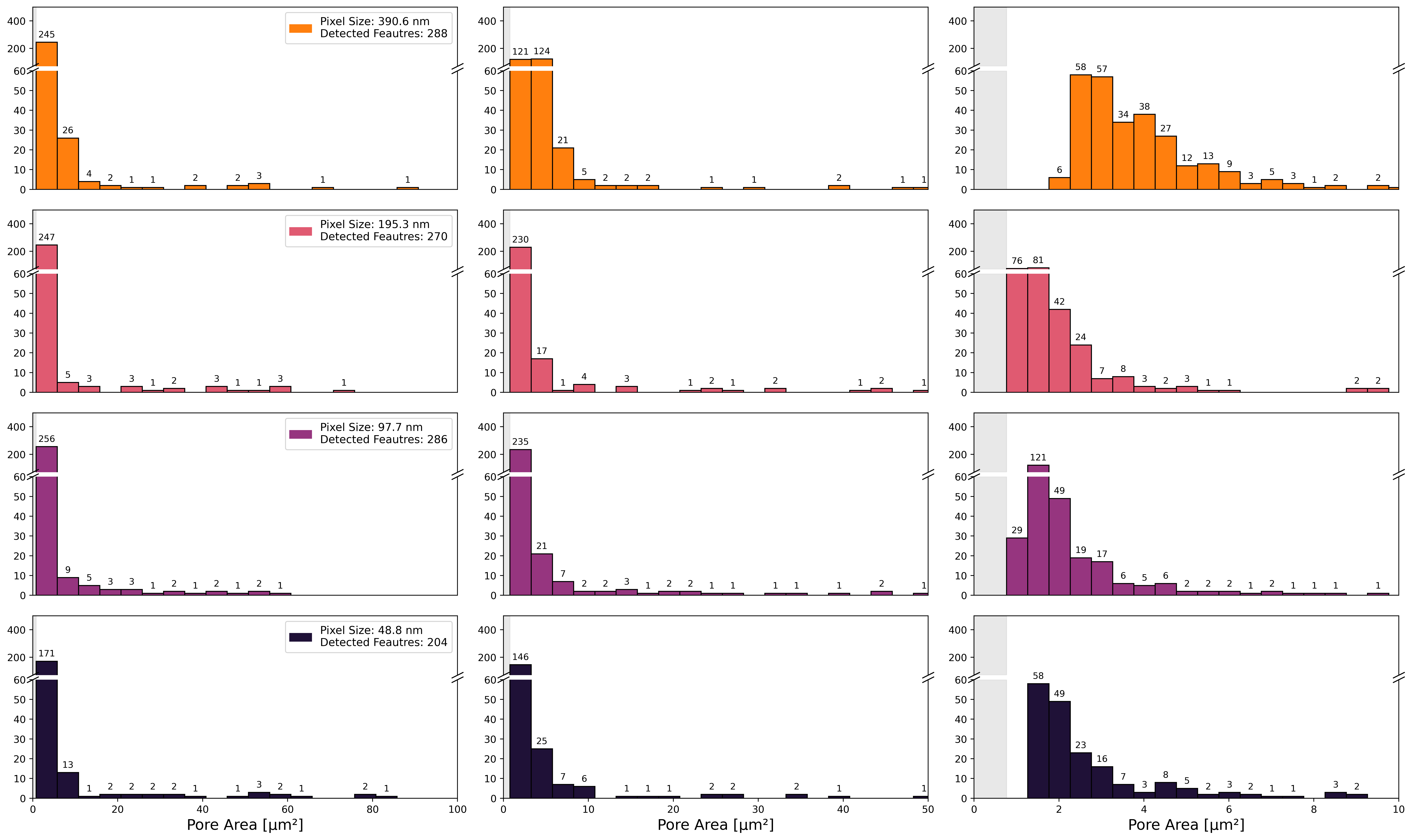
Figure 3.3:Histograms for defect area distribution at varying pixel sizes, a) overall distribution with 5 µm² bin size, b) 0–50 µm² range with 2.5 µm² bin size, and c) 0–10 µm² range with 0.5 µm² bin size. Gray areas show cut-off regions due to the 5-pixel size constraint imposed by the minimum feature size of the dataset acquired with a pixel size of 390nm.
Increasing the pixel size from 48 nm to 390 nm influences the distribution of detected defect sizes, particularly within the 0–5 µm² range. The histograms in Figure 3.3 illustrate how the representation of defect size changes with pixel size. Figure 3.3 (middle) highlights the range from 0–50 µm², while Figure 3.3 (right) focuses on defect sizes between 0–10 µm². At smaller pixel sizes, the defect size distribution is skewed toward smaller values, with a sharp decline in counts beyond 5 µm². In contrast, at larger pixel sizes, the defect size distribution appears broader, particularly in the mid-size range of 5–10 µm² (Figure 3.3–right). This broader distribution at larger pixel sizes may be attributed to the reduced spatial resolution, which impacts the precision of defect boundary detection. As pixel size increases, the intensity value of a pixel represents the average signal over a larger area, smoothing out subtle contrast differences that are essential for precise boundary definition. Consequently, defect boundaries become less well-defined, making it more challenging to classify boundary pixels accurately. This effect can artificially inflate the apparent size of certain defects, skewing the distribution toward larger values, particularly in the 2.5–10 µm² range.
To mitigate these effects, further refinement of detection parameters or the introduction of additional constraints in the algorithm may be necessary. However, the defect size distributions for the lower pixel sizes (48 nm, 97 nm, and 195 nm) appear quite similar, suggesting that the impact of pixel size on the detected size distribution is more pronounced at larger pixel sizes.
Effect of Dwell time
To assess the impact of reduced SNRs on defect detectability due to a reduced dwell time using our framework, the SEM micrograph corresponding to a dwell time of 10 µs and a pixel size of 195.31 nm was used as the benchmark throughout this entire section. The effect of reduced dwell time was assessed by calculating the PSNR using reference data obtained at a dwell time of 10 µs. PSNR measures the similarity between test and reference images, with higher values indicating greater resemblance and therefore, lower noise levels. Figure 3.4 illustrates the relationship between dwell time and PSNR values fitted against a square root function.
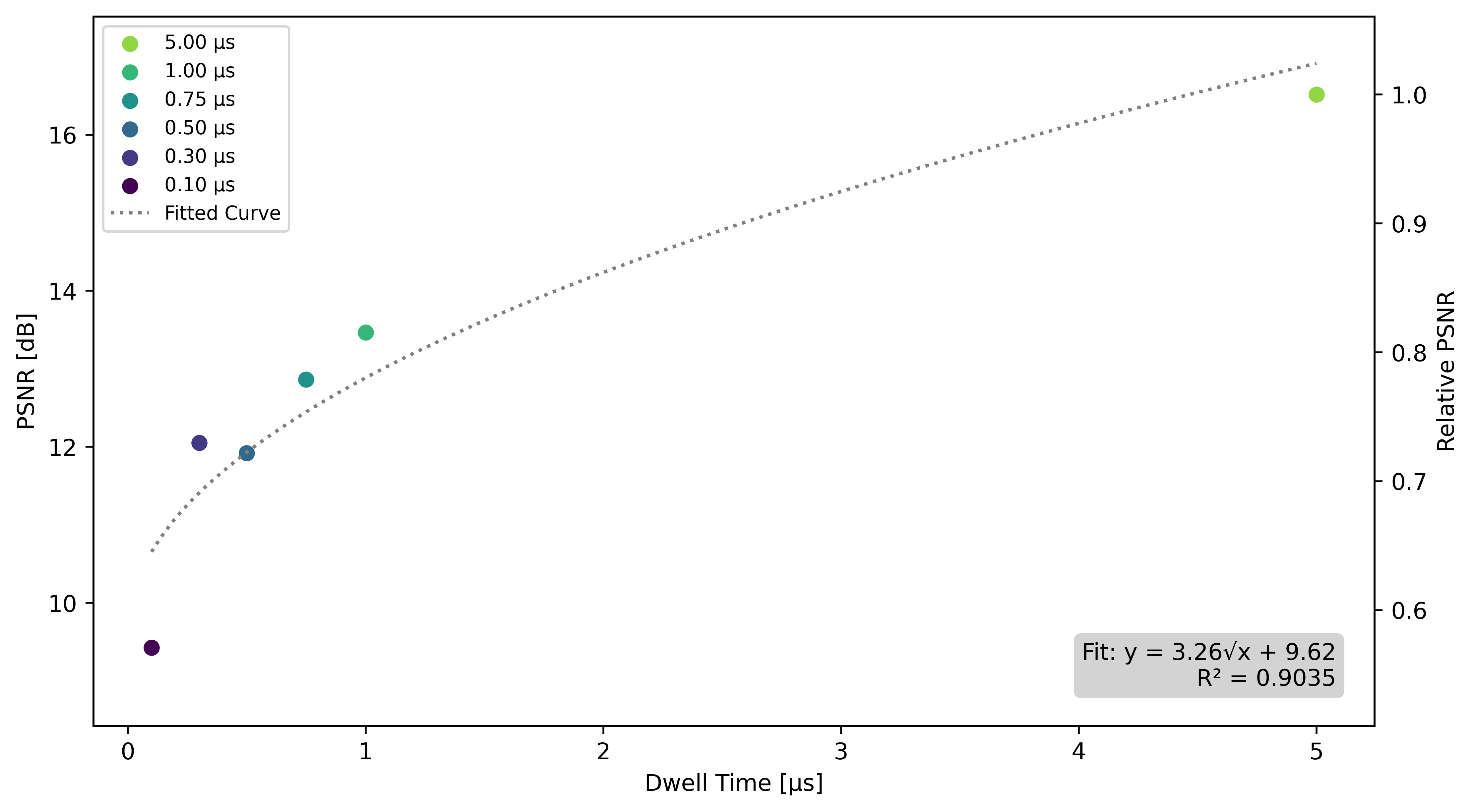
Figure 3.4:Relationship between dwell time and PSNR, with values calculated relative to a 10 µs dwell time benchmark and fitted to a square root function.
PSNR values exhibit a non-linear decrease as dwell time decreases. Reducing the dwell time from 5 µs to 1 µs causes the PSNR to drop from 16.5 dB to 13.5 dB, which corresponds to a relative drop of 20 %, from 1 to 0.82. Reducing the dwell time by a factor of 2 to 500 ns, leads to a PSNR of 11.9 dB, or a relative value of 0.72, representing another 10 % reduction in image quality. At the shortest dwell time of 100 ns, the PSNR reaches a minimum of 9.4 dB, the lowest level observed, showing the weakest agreement with the reference image captured at 10 µs. This corresponds to a relative drop of 43% compared to the higher dwell time of 5 µs.
According to Joy, 2008, noise in SEM scales with the square root of the mean electron count M. As dwell time increases, the mean count rises, but noise increases more gradually, only as . Consequently, at longer dwell times, PSNR improvements become less pronounced, leading to a non-linear trend where additional dwell time yields only marginal gains in the PSNR. This relationship is captured in Figure 3.4, where the fitted curve follows a square root function, achieving an R² value of 0.9 and indicating strong agreement with the observed PSNR values.
AAA values and Error rates relative to the benchmark were determined for each dwell time, as shown in Figure 3.5. All micrographs were captured with a consistent pixel size of 195.31 nm. The effect of varying the filtering constraint on AAA and Error was analyzed for values of ten and fifty.
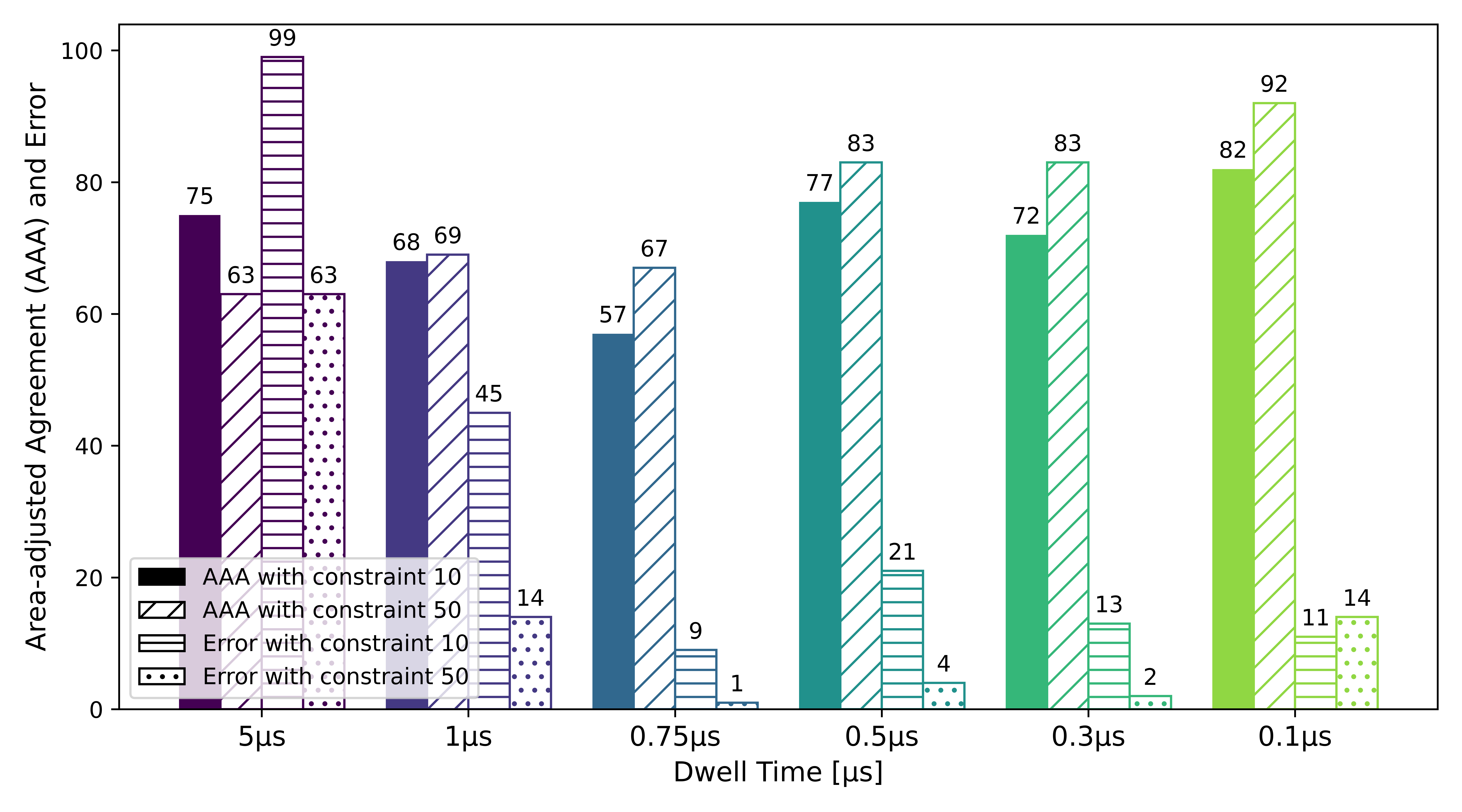
Figure 3.5:Overall AAA and error relative to highest dwell time results.
Applying a minimal filtering constraint of 10 (the product of area * roundness values is above the constraint - as defined in Assessment of defect detection - corresponds to a value for AAA of 82 % at a dwell time of 5 µs, indicating a slight reduction in agreement with the reference. However, increasing the filtering constraint to 50 raises AAA to 92%. This trend persists at shorter dwell times: at 1 µs, AAA is 72% for a constraint of 10 and 83% for a constraint of 50. The difference becomes even more pronounced at lower dwell times, such as 500 ns, where AAA reaches 57% for a constraint of 10 and 67% for a constraint of 50.
At high dwell times, such as 5 µs, Error remains low - primarily caused by smaller defects, with values of 11% for a constraint of 10 and 14% for a constraint of 50, indicating that most detected structures correspond to actual defects rather than noise. As dwell time decreases, Error rates increase, suggesting that not only large defects are captured but also a growing amount of noise, which becomes mistakenly classified as small defects – this is especially true when using the minimum constraint of 10 instead of 50. At 1 µs, for example, Error rises to 13% for a constraint of 10 and 2% for a constraint of 50. This trend continues at even lower dwell times, reaching 21% at 750 ns and 57% at 500 ns for a constraint of 10. At 100 ns, Error values become exceptionally high, peaking at 99% for a constraint of 10 and 63% for a constraint of 50. In these cases, high AAA values can be misleading, as much of the agreement is driven by random noise rather than true defect detection. Error rates for a filtering value of 50 remain consistently lower than those for a constraint of 10, as the higher threshold effectively removes noise while still capturing most true defects. However, setting the filtering constraint too high may also exclude valid defects, artificially inflating Error rates by reducing the number of matching features between the benchmark and low dwell time images.
This trade-off between filtering constraints and defect detectability highlights the importance of considering not just AAA alone but also the balance between agreement and Error. While increasing the filtering constraint helps suppress noise and improve agreement with the benchmark at higher dwell times, its effect is more complex at lower dwell times, where high Error rates can undermine the reliability of AAA as a standalone metric. In such cases, the difference between AAA and Error (i.e. AAA - Error) provides a more meaningful measure of detection performance, as it accounts for the extent to which noise contributes to apparent agreement.
The relationship between PSNR and AAA - Error for a filtering constraint of 10 is examined in Figure 3.6a), assessing how increasing noise at different dwell times impacts detection accuracy. As PSNR values rise, a corresponding increase in AAA - Error is observed, indicating a dependency. A Pearson correlation analysis was conducted to quantify this relationship despite the limited number of data points. The analysis yielded a high correlation coefficient of 0.869 (p = 0.025), confirming the statistical significance of the observed trend.
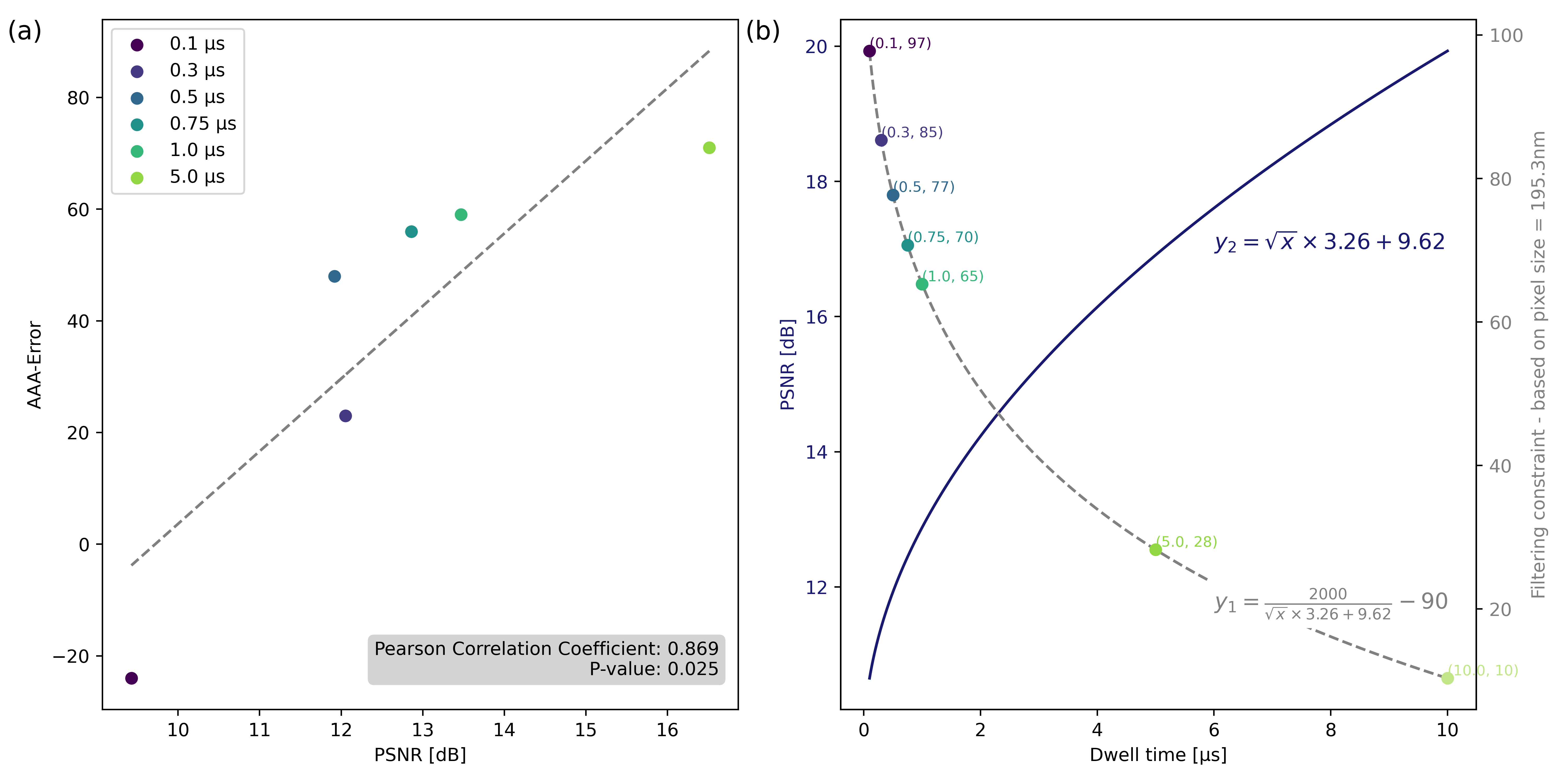
Figure 3.6:a) PSNR values at varying dwell times vs. AAA - Error, showing a linear correlation (Pearson coefficient = 0.869, p=0.025), b) PSNR trend (blue) and filtering constraint function (gray) as functions of dwell time
While this relationship demonstrates the reliability of higher PSNR values in improving agreement, it also reveals limitations in the algorithm’s sensitivity to noise and artifacts at lower PSNR values. Underscoring the importance of carefully selecting threshold values based on image quality, defect characteristics, and the noise level present in the dataset.
Therefore, a thresholding/filtering approach, inversely dependent on the PSNR trend, is implemented to improve feature recognition under varying noise conditions to counteract this effect. The values as presented in Figure 3.6b) correspond to our benchmark pixel size of 195 nm, to which all other detections were scaled. Given this trade-off, the analysis provides guidance on acceptable PSNR thresholds for determining required dwell times, while acknowledging known defect detection limitations.
Combined effects of dwell time and pixel size
The interplay between dwell time and pixel size significantly influences defect detection accuracy, as both parameters contribute to the resolution and noise characteristics of acquired images and need to be carefully balanced. Comparisons between the PSNR dependent filtered datasets and the benchmark dataset are presented as heat maps in Figure 3.7. The left panel displays AAA, reflecting the retention of defect information, while the right panel shows Error rates across the acquisition parameters.

Figure 3.7:Heatmaps displaying the AAA Value Matrix (left) and Error Value Matrix (right) across varying pixel sizes and dwell times. The matrices highlight the distribution of values against the benchmark dataset with a pixel size of 195nm and dwell time of 10µs. Note: due to the high Error value for the datasets of a pixel size of 391nm for 100ns and 300ns, these are excluded from the applied color scale
As expected, detection accuracy is highest at smaller pixel sizes and longer dwell times, as shown in the AAA matrix (Figure 3.7, left), which exhibits an increasing trend in AAA values from the top left (low dwell times and larger pixel sizes) to the bottom right (high dwell times and smaller pixel sizes). AAA decreases sharply as dwell time is reduced, particularly for larger pixel sizes. For example, at a dwell time of 1 µs, the AAA for a pixel size of 195 nm is 85, but it drops to 74 for a pixel size of 391 nm. At the shortest dwell time of 100 ns, smaller pixel sizes such as 49 nm retain a high AAA of 100, whereas larger pixel sizes, such as 391 nm, AAA declines significantly to 43. This demonstrates that larger pixel sizes are more susceptible to the combined effects of reduced resolution and increased noise at shorter dwell times. In contrast, smaller pixel sizes maintain higher AAA values under these conditions due to their superior spatial resolution and greater resilience to noise. However, this comes at the cost of significantly longer acquisition times, which limits its practicality for high-throughput applications.
The high AAA values (>100%) observed at small pixel sizes and long dwell times, such as 49 nm, can again be attributed to bright edge effects in the SE images, which are more pronounced at smaller pixel sizes, where the detector’s ability to capture subtle topographical changes is amplified.
Error rates (Figure 3.7, right) show a similar trend. For instance, at a pixel size of 391 nm and a dwell time of 100 ns, Error rates rise extremely to 93 %, highlighting the higher susceptibility of larger pixel sizes to noise artifacts. These artifacts lead to false defect detections and inflated defect areas, reducing the reliability of defect characterization. In contrast, smaller pixel sizes exhibit minimal Error even at shorter dwell times, further reinforcing their accuracy advantage.
These findings emphasize the trade-offs between acquisition speed and detection accuracy, particularly in large-area scans. While larger pixel sizes and shorter dwell times reduce acquisition times, they also increase noise-related artefacts and result in the loss of smaller defects, potentially skewing defect distribution analysis. Notably, noise from lower dwell times tends to have a greater impact on AAA than resolution from pixel size alone. However, by carefully selecting specific dwell time and pixel size combinations, it is possible to minimize these trade-offs, achieving a balance between acquisition speed and detection accuracy. For example, certain parameter combinations enable a significant reduction in acquisition time while maintaining similar accuracy. A pixel size of 195 nm with a dwell time of 5 µs results in an AAA value of 84 while decreasing the dwell time to 1 µs at the pixel size results in an AAA of 85 with a slightly reduced Error rate (from 13 % to 0 %) while significantly reducing the relative acquisition time. This demonstrates that acquisition time can be optimized by approximately a factor of 5 while still maintaining sufficient defect detectability with a known uncertainty limited by the applied filtering constraints.
Additionally, dwell time and pixel size are not the only factors influencing acquisition efficiency. An analysis of the estimated acquisition times in Table 2.1 reveals that reducing dwell time does not scale proportionally with the overall reduction in acquisition time. For example, with a pixel size of 195.3 nm, decreasing the dwell time from 1 µs to 0.5 µs reduces the relative acquisition time from 13% to 10%, rather than the expected halving. Further reductions to 0.3 µs and 0.1 µs result in only marginal decreases to 9 % and 8 % respectively. This indicates that the fixed speed of the microscope stage movement is an additional factor to consider when trying to optimize acquisition time versus detection accuracy.
Effect of Noise Reduction on Defect Detection Accuracy
To address the decrease in the value of AAA observed at low dwell times, the HR-SEM denoising approach proposed by Lobato et al., 2024 was assessed to denoise SEM large-area micrographs. Figure 3.8 illustrates the number of defects in correspondence after adaptive filtering values as presented above were applied, comparing valid defects in the datasets as acquired and after denoising. All micrographs were acquired with a pixel size of 195 nm.
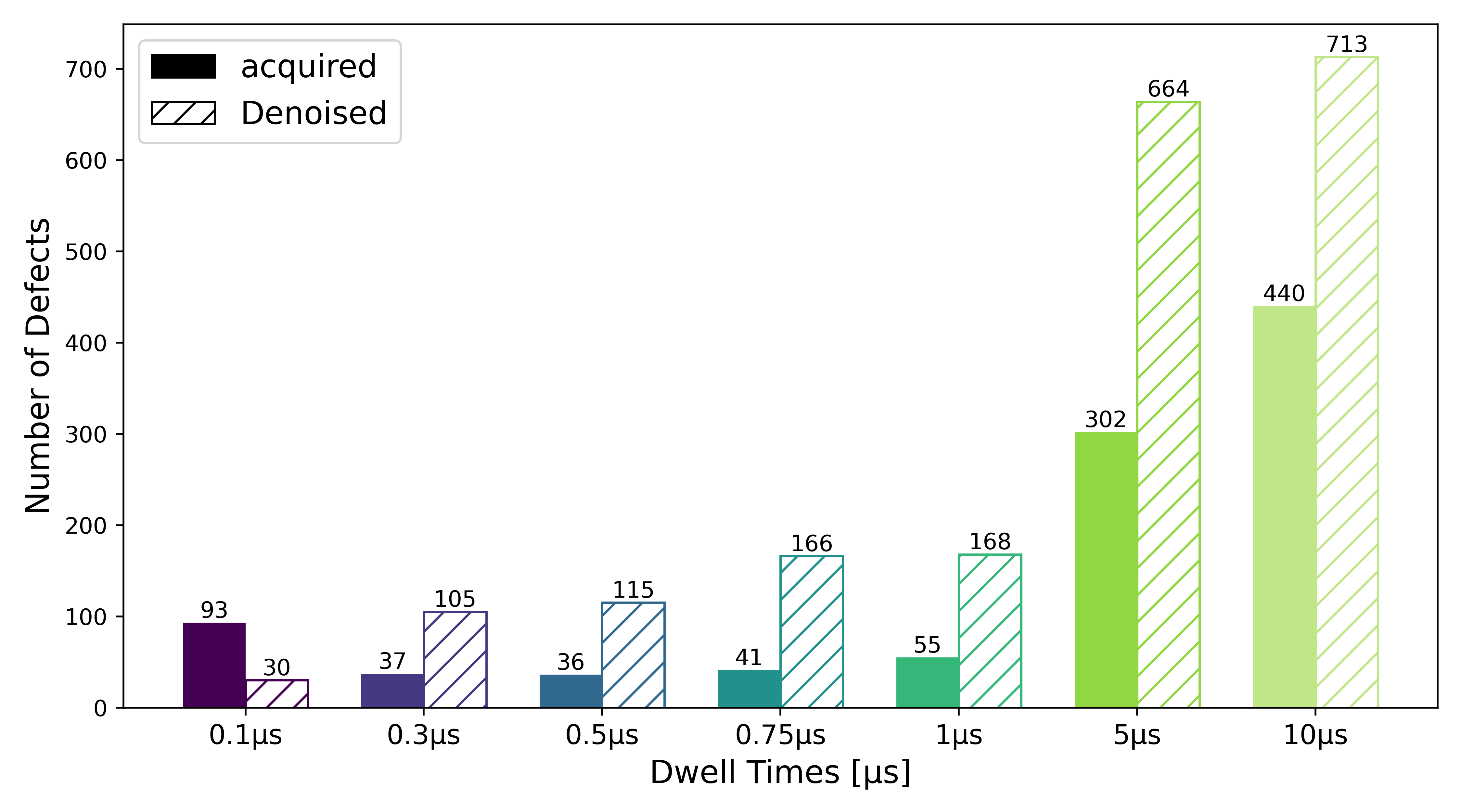
Figure 3.8:Number of defects detected in acquired and denoised SEM datasets across dwell times, adaptive filtered values in dependency of dwell time are applied
At most dwell times, denoising results in an increase in the number of detected defects after applying the filtering constraints, increasing the number of overall defects detected closer to the benchmark dataset. For instance, at 5 µs, the defect count increases from 302 in the acquired dataset to 664 after denoising. Even at lower dwell times, for instance, at 300 ns, the number of defects increases from 37 in the acquired dataset to 105 after denoising. This suggests that the process not only removes noise but may also enhance the detectability of features that meet the filtering criteria. Denoising may improve the roundness or clarity of features, making them more likely to pass the filtering process. This indicates that denoising at lower dwell times helps detect features that might otherwise be masked by noise.
A direct comparison of AAA and Error rates between the as-acquired micrographs Figure 3.7 and their denoised counterparts (Figure 3.9) is presented. Both figures use the same benchmark dataset, ensuring a consistent basis for evaluation. The color scale remains identical across both figures.

Figure 3.9:Heatmaps displaying the AAA Value Matrix (left) and Error Value Matrix (right) for denoised datasets across varying pixel sizes and dwell times. The matrices illustrate improvements in AAA and changes in Error rates compared to the as-acquired benchmark dataset with a pixel size of 195 nm and dwell time of 10 µs
Denoising effectively reduces noise artifacts, enhancing image clarity and improving the detection of larger or more pronounced defects, especially at shorter dwell times and larger pixel sizes where noise effects are more pronounced. For instance, at a pixel size of 98 nm and a dwell time of 1 µs, the denoised dataset achieves an AAA of 106 (Figure 3.9 – left), compared to an AAA of 71 in the as-acquired dataset. Similarly, at a pixel size of 391 nm, the AAA improves from 74 to 100 by denoising.
However, this improvement comes with a trade-off: in some cases, denoising increases the overall Error rate compared to the as-acquired dataset. This effect arises due to two primary factors. Denoising amplifies edge effects around larger defects, leading to crescent-shaped artifacts that are mostly absent in the raw images. These artifacts introduce additional false detections, increasing the overall Error rate. At larger pixel sizes, denoising can further impact defect detection by suppressing small features. While it effectively reduces noise and prevents false positives, it also smooths out fine details, making subtle defect indicators less distinguishable. This effect is particularly noticeable at a pixel size of 195 nm and a dwell time of 500 ns, where the Error rate in the denoised dataset increases to 29, compared to 0 in the as-acquired state. Conversely, at smaller pixel sizes, where higher spatial resolution preserves fine details and local contrast variations, denoising is more beneficial. For instance, at a pixel size of 49 nm and a dwell time of 100 ns, the Error rate decreases from 34 in the as-acquired dataset to 28 in the denoised one.
Lastly, the impact on the overall analysis time must be considered. Larger pixel sizes reduce the number of pixels per image, leading to a decrease in analysis time. However, this benefit is partially offset by additional image processing steps, such as denoising and edge correction, which may introduce slightly longer computational time. These post-processing steps are especially critical when working with larger pixels, as noise artifacts and resolution loss can otherwise lead to significant misclassification of defect features. Consequently, while reducing pixel density can accelerate data collection, the trade-off in post-processing steps must be evaluated depending on the specific application requirements.
Effect of high-throughput acquisition approach on Key defect descriptors in model sample
In the previous sections, the analysis focused on how variations in image acquisition settings influence the values of AAA and Error. However, for AM samples — with AM steel as the model system — certain feature descriptors such as roundness and orientation relative to the baseplate and print direction are particularly important for understanding how manufacturing process conditions influence defect formation and part quality. To evaluate whether optimizing for shorter image acquisition times affects these descriptors, three datasets were selected. Each dataset meets the criteria for achieving an AAA above 80 and an Error rate below 15%, while providing improved acquisition times compared to the benchmark dataset.
Figure 3.10 presents bubble plots illustrating the relationship between the area of defects and their roundness, depending on the selected image acquisition conditions. The size of each bubble represents the number of defects detected in that bin, normalized by the total number of defects for each acquisition parameter. A roundness threshold of 0.3 was implemented, as roundness serves as an indicator of defect type, distinguishing more rounded pores from elongated cracks. The same filtering values as those used in Figure 3.7 and Figure 3.9 were applied and are visualized by a gray background.

Figure 3.10:Bubble plots showing defect area (log scale) vs. roundness under different image acquisition conditions. Cracks (blue) and gas pores (green) are differentiated by a roundness threshold of 0.3. Total acquisition time is decreasing from left to right.
As acquisition time decreases from a dwell time of 10 µs with a pixel size of 195 nm (benchmark, 100 %) to a dwell time of 500 ns and a pixel size of 98 nm (41 %) and finally a dwell time of 1 µs and a pixel size of 195 nm (13 %), changes in defect detection become noticeable. Figure 3.10 shows that in the as-acquired datasets, the detection of smaller defects decreases as acquisition time is reduced. This effect is due to the filtering constraints, which eliminate the smallest detected features to reduce noise-related artifacts (see gray areas indicating the filtering constraint). As a result, a greater proportion of small pores may be excluded from datasets acquired with shorter dwell times, leading to an apparent reduction in the number of detected defects in the lower-area bins. Despite this, the overall distribution of pores remains similar between 500 ns – 98 nm and 1 µs – 195 nm, suggesting that, within this range of acquisition settings, defect detection remains relatively stable.
The dataset which includes denoising highlights how noise reduction enhances defect detection accuracy. Compared to the as-acquired dataset, AAA increases from 91 (Figure 3.7) to 105 (Figure 3.9) while Error also increases substantially from 2 to 14.
Although denoising increases defect retention, bubble plot analysis (Figure 3.10) shows that it also causes a shift in defect distribution compared to the benchmark. A larger number of defects with higher roundness values are detected, as boundary smoothing reduces jagged edges and irregularities. While denoising improves detectability, it also slightly inflates roundness values, making defects appear more circular than in the as-acquired state. This effect must be considered when analyzing defect morphology, as it may influence the interpretation of defect shape and classification.
Another key aspect in analyzing defects in AM samples is the orientation or elongation of defects relative to the baseplate and print direction, which provides insights into process parameters and solidification conditions. This analysis examines the impact of imaging acquisition parameters on pore orientation. To ensure reliable measurements, specific constraints are applied: only pores with roundness values between 0.3 and 0.6 are included, as highly circular defects tend to have arbitrary orientations.
The following rose diagrams (Figure 3.11) illustrate the distribution of pore orientations across the selected imaging conditions. In these diagrams, the horizontal axis represents the baseplate reference: 0° corresponds to defects aligned parallel to the build plate, while 90° indicates defects oriented perpendicular to it.

Figure 3.11:Angular distribution of defect orientations in dependency of image acquisition conditions, with decreasing acquisition time from left to right.
In the benchmark dataset, the highest number of features is detected, with the rose diagram showing a relatively uniform distribution of defect orientations across a broad range of angles, without distinct clustering. At a pixel size of 98 nm and a dwell time of 500 ns, the dataset reveals a significantly reduced number of detected defects compared to the benchmark. The detected defects predominantly exhibit flatter angles, as indicated by the narrower distribution of orientations in the rose diagram. One possible explanation is that the shorter dwell time hinders the detection of finer structural features, particularly those with distinct shapes. In contrast, the dataset of 1 µs – 195 nm shows an orientation distribution trend very similar to the benchmark dataset, though it consistently detects fewer defects.
However, after denoising, the dataset shows a shift in orientation trends. It contains the fewest detected features and displays the narrowest, most refined orientation distribution. Unlike the more uniform defect distribution in the benchmark dataset, defects in the denoised dataset predominantly cluster around 70°. This clustering may be associated with an increase in roundness values due to the denoising process, as seen in Figure 3.10. By eliminating noise and smoothing defect shapes, denoising makes defects appear more circular. As a result, their orientation becomes less meaningful or reliable, potentially leading to an apparent clustering at specific angles, such as 70°.
- Joy, D. C. (2008). Noise and Its Effects on the Low-Voltage SEM. In Biological Low-Voltage Scanning Electron Microscopy (pp. 129–144). Springer New York. 10.1007/978-0-387-72972-5_4
- Lobato, I., Friedrich, T., & Aert, S. V. (2024). Deep convolutional neural networks to restore single-shot electron microscopy images. Npj Computational Materials, 10(1). 10.1038/s41524-023-01188-0
