Nanocartography: Planning for success in analytical electron microscopy
Practical Applications of Nanocartography
4.1Calibration of the Double Tilt Stage
The premise of utilizing nanocartography for electron microscopic analysis centers on the knowledge of the α and β axes of a double tilt stage (note: as described in Navigation and Orientation, the α,β convention is equivalent to X and Y tilt axes). A similar procedure can be performed for a single tilt stage, but it precludes much of the information that can be collected (i.e., the ability to tilt within a crystal and stage motion are limited to one axis). The power of utilizing these techniques is that once the spatial relation of the α and β tilt axes are known for a specific microscope (note that the β can be simply deduced as orthogonal to the α once it is determined), any information gathered from a sample can be translated in any fashion for use on another microscope as long as the tilt axes have been similarly calibrated. This information allows any microscopist to perform routine pre-screening of data regardless of time or peripherals on any microscope before either reanalyzing the sample in the same microscope, or transferring it to a different facility or scope with more advanced capabilities.
The simplest manner in which to calibrate the α axis in imaging modes is through the use of a carbon contaminated sample. Once loaded, a region of interest that appears to be relatively uniform and flat should be selected. Carbon mounds on both the top and the bottom of the sample can be produced by condensing the beam to a fine point over the region (Figure 4.1). After a set amount of time, the probe can be defocused to detect whether carbon mounds were produced. Once a sufficient amount of cracked carbon has been deposited, an image at α,β:0,0 can be collected for reference (Figure 4.1a). The sample should then be tilted approximately both positive and negative 10˚ in the α, at which tilt point images should be collected. From the three images collected, the circular projection of the carbon mound at α,β:0,0 should become elliptical at both positive and negative α tilts. The long axis of the elongation is the α tilt axis. For the β axis, one can either draw a line orthogonal to the α or repeat the procedure of starting at α,β:0,0 and tilting to positive and negative 10˚ in the β to ensure the correct location of the axis. The calibration of the α axis needs to be performed at tilt condition α,β:0,0, from which the subsequent calibration across tilt space can be applied (e.g., at tilt conditions farther from 0,0 the actual α will be some mathematical rotation from the calibration at 0,0 depending on location).
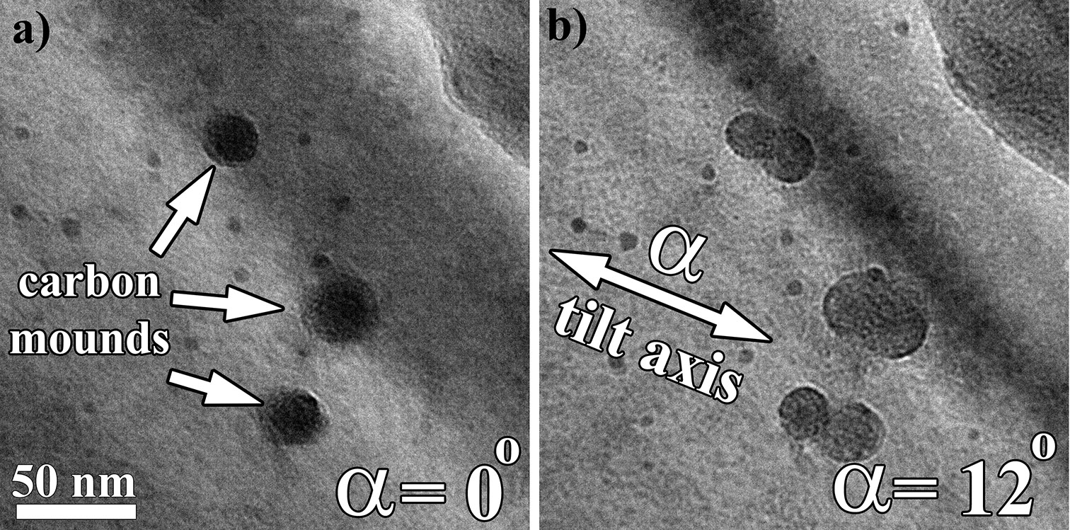
Figure 4.1:TEM (BF) images showing carbon contamination (mounds) deposited on a sample (a), followed by a pure α tilt to highlight orientation of the α tilt axis (b). For all other tilt calculations in TEM (BF) mode the angle to the α axis will be measured from this line.
As previously demonstrated in Practical Derivations, the calibration of TEM diffraction and STEM (Ronchigram) modes can be performed with any crystalline sample, preferably one with larger, single crystals as the calibration will be performed utilizing the position of diffraction discs and Kikuchi lines emanating from a single source (Figure 4.2). In either TEM diffraction mode or Ronchigram mode, a grain should be selected that is relatively close to a zone axis (ZA) when the stage is at α,β:0,0. The grain should be uniformly flat and set at the eucentric height. This procedure works best if a grain oriented close to a higher index ZA grain is selected since the systematic reflections intersecting at the ZA will provide a good fiduciary marker (too low an index could skew the visibility of the center of the ZA). Using a large condenser aperture (preferably in CBED mode if the microscope allows it), the probe should be condensed to a point followed by subsequent analysis in diffraction mode. A center fiduciary image can then be taken with the oriented ZA as the nominal zero position (Figure 4.2a and c). The sample should then be tilted approximately ±5˚ in the α at which time an image should be taken (Figure 4.2b and d). From each image collected a trace of the center of the ZA can be drawn, hence providing a measure of the α tilt axis. As with the calibration of the TEM bright field and STEM imaging conditions, the β tilt can be ascertained as orthogonal to the α tilt axis, or the aforementioned protocol can be repeated using the β tilt in place of the pure α tilts.
Depending on the sample thickness, the observation of the Kikuchi lines intersecting at a high index ZA are the easiest to observe. The same procedure can be used in parallel beam diffraction mode, except the center of the ZA needs to be identified by tracing a circle intersecting the Ewald sphere and determining the center of the circle to pinpoint the ZA. This approach can be more difficult and is less favorable than using Kikuchi lines. In diffraction mode the orientation of the α tilt axis can corroborated by defocusing the diffraction pattern either over or under focus (Figure 4.2e and f, respectively) to observe the physical relation of the diffraction pattern to the sample.
Lastly, a large, relatively flat single crystal can be used to calibrate the α tilt axis using two ZA and the methodology formulated to solve unknown crystals. Figure 4.3 illustrates selected area diffraction (SAD) patterns of two ZA ((a)<110> and (b)<112>) of a CuNi alloy, of which the details of the alloy are provided in subsequent sections and in the Appendix. The tilt coordinates of each of the found ZA is shown in Figure 4.3c. The angle necessary to connect these two ZA will correspond to a specific g-vector in the diffraction pattern, in this case the {111} vector connects the <110> and <112> and the angle from the α tilt axis is 6°. Therefore, in the SAD patterns an angle orthogonal to the measured angle in Figure 4.3c (i.e., angle +/- 90° due to the Kikuchi band being orthogonal to the g-vector) will illustrate where a fiduciary marker for the α tilt axis can be measured for all diffraction patterns. As the projection of the lattice planes will rotate slightly at oblique angles, the use of the unknown calculator will accurately account for the measuring and plotting traces between ZA. This is the exact reasoning for why diffraction patterns collected across the entire tilt stage require slight rotations by which to keep the g-vectors aligned. The S-curves illustrated in Navigation and Orientation represent the angles by which the planes rotate.
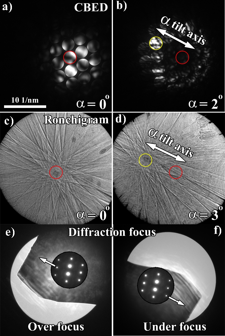
Figure 4.2:Calibration of the orientation of the α tilt axis in TEM diffraction and STEM (Ronchigram mode) using a single crystalline sample. CBED patterns (a-b) illustrate the crystal on zone (a) and tilted ~2° in the α tilt (b). Ronchigram mode showing the crystal on zone (c) and ~3° in the α tilt (d). Over (e) and under (f) focus images of the central diffracted beam showing the orientation of the sample with respect to the diffraction pattern.
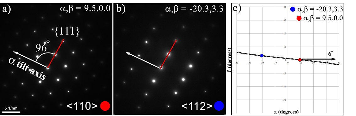
Figure 4.3:Calibration of the alpha tilt axis using a single, locally flat sample. SAD patterns (a,b) were collected at various tilt conditions and then plotted (c) to obtain an approximate measurement of the α tilt axis.
Once each mode is calibrated for the location of the tilt axes, it is suggested that digital templates be created for future analysis by which to overlay and measure data currently being collected. The most important is the orientation of the α tilt axis because every measurement moving forward in these protocols are measurements to this axis. The β could similarly be used except that the default is to the α because it is typically the most eucentric of the two axes. In order to best be able to utilize these protocols, it is necessary to be able to measure the radial angle between the α axis and a given fiduciary, whether it be a diffraction spot, Kikuchi line, or interface. As noted in Pracitcal Derivations, these calibrations can be incorporated into an algorithm utilizing digital capture in order to use the computer screen to perform small angle tilting of the sample.
4.2Tilt Stage Limit
In order to understand the limitations of the tilt map produced for any number of operations, it is necessary to calculate and map out the limit of the stage motions Olszta et al., 2022. This can be achieved by assuming symmetry of the stage motion and tilting to a set number of α tilts and then determining the corresponding limit of the β tilt. When mapped on the JEOL ARM200CF the standard double tilt holder has the shape of a “squircle” or superellipse. The superellipse is defined by:
Where α and β are the tilt stage readouts, a and b are the α and β tilt limits, respectively, and r is a shape factor. Figure 4.4 is a plot illustrating stage limits of a =36 and b = 32 for a number of shape factors with an r value of ~3.3 used a good description of the JEOL double tilt holder for the ARM200CF. While these tilt limits can be programmed as look up tables to curtail outputs (e.g., when plotting specific crystals or for calculating tilt series calculations) the ability to trace Kikuchi bands outside of the tilt limit can be beneficial to understanding crystallographic data of an unknown sample.
HBox(children=(Canvas(footer_visible=False, header_visible=False, layout=Layout(width='470px'), resizable=Fals…
Figure 4.4:Double tilt stage limits as calculated through a squircle (superellipse) estimation using various r values.
4.3Crystallographic Orientation
The calculations and derivations of formulae surrounding crystallographic orientation using a double tilt stage have already been presented, but a more practical discussion of how to apply these techniques can be discussed. First, it is necessary to have a general understanding the movement of the double tilt stage in comparison to a pole figure or stereographic projection (see Figure 2.4). Whereas the planes of traces of atoms in a stereographic projection appear to move in a straight or arced path, in the tilt map the planes move in an S-curve fashion due to the α,β relationship. For instance, with a cubic crystal positioned with the [001] at the α,β:0,0 tilt coordinates and the [100] along the α or β orientation, the tilt conditions for the [111] will be observed by first tilting alpha to 35.3° and then beta to 45°, but the reverse order (beta to 35.3° and then alpha to 45°) will not because of the dependency of the order to the stage motion. Utilizing this allows orientation of any crystal using the following protocols.
With experience and familiarity with a single system, microscopists can eventually identify diffraction or Kikuchi patterns from memory, and eventually identification of each plane within the diffraction pattern becomes second nature. However, for inexperienced users identifying these crystallographic waypoints can be a challenging if not daunting experience. It should be noted that the work Xie et al. has automated this in an open source manner Xie & Zhang, 2020, but for completeness the protocols will be provided here.
In order to optimize crystallographic solutions with regard to the sample and stage, at least one known or identified pole must be determined as a proposed starting point. The stereotypical, six-fold symmetry of a <111> cubic crystal is presented at stage positions α,β:10.9,5.0 (Figure 4.5). Depending on the level of confidence with the found pole, the next step is to either tilt to a second known pole somewhere within the tilt stage to set a second waypoint or to follow orient to a known g-vector.
Since the preliminary calculations of the crystallographic solution are based upon the first known pole (e.g., <111>) the remainder of the crystal will rotate concentrically about that pole. Given the crystallographic system has already been identified, the crystal can be rotated about the first pole until a second proposed pole lines up with the tilt conditions of the second pole. For instance if a second pole were discovered at α,β:13.3,-14.8 the crystal could be rotated until the <112> type pole would line up. Depending on the confidence of the user in the identification of the two known poles and the symmetry of the crystal system, a third and final pole could be identified on the map and confirmed by tilting to that point (e.g., the <110> type at -16.6, -17.3). For mapping and predictive tilting of the sample, the symmetry of the given crystal system is not as important in setting this rotation correction. When considering the orientation relationship between two grains (i.e., misorientation angle) it is necessary that the directionality of each adjacent grain be considered.
For more experienced microscopists, measuring the angle of a known plane to the α tilt axis angle can be utilized in combination with the first known pole. In Figure 4.5 the {110} is measured ~20º to the α tilt axis and can then be adjusted accordingly in the tilt map to get the projection of the {110} correct. Again, depending upon the symmetry of the crystal system, other poles can be located and tilted to in order to confirm the orientation. Once enough poles have been identified to satisfy the correct orientation, the crystallographic solution for that crystal has been mapped and can be utilized for future tilt experiments and the determination of vector normals to interfaces and adjacent grains. This is extremely important for inexperienced users to gain familiarity with a crystal system, as a large number of poles can be quickly visited thereby building up experience with that crystal type. For this reason alone, for less experienced users this is more beneficial than an automated system of which it may be tempting to blindly trust the output. Automation can be a powerful, but without a proper understanding of the underlying principles, it can be improperly used.
As shown in Figure 4.5, the collection of a CBED or Kikuchi map makes this exercise trivial because the measured angle to the α tilt axis can be quickly, efficiently, and accurately measured. This does not preclude microscopists without the ability to collect such pattern from utilizing these methods. Once two known poles have been identified, the tilt positions of the poles can be used to calibrate the crystallographic solution similar to the aforementioned protocol. The poles/planes of the entire crystal can then be traced and visited.
Mapping of crystals in this manner can be extremely useful in confirming suspected crystals as well as rapid tilting for collecting diffraction or atomic column images. Depending on the crystal, one pole may have a unique projection of atomic planes that helps identify specific atomic positions. For instance, in dislocation contrast imaging (DCI) the <110> is a preferential pole in FCC materials to indicate a large basis set of {111} planes Zhu et al., 2018Phillips et al., 2011Sun et al., 2019. Understanding the exact location of the <110> within a specific crystal could suggest that the sample is too thick (i.e., a large tilt condition) to achieve clear dislocation images. It would allow a microscopist to then either find an additional crystal or tilt to a less desirable pole. Lastly, when presented with opportunity to utilize a crystallographic solution, microscopists could more confidently confirm the specific crystal and avoid misidentification by rapidly tilting to multiple poles. This type of analysis would not only be beneficial for assuaging scientific reviewers, but would again be most beneficial to inexperienced users who are not accustomed to rapid identification of specific poles through fingerprinting.
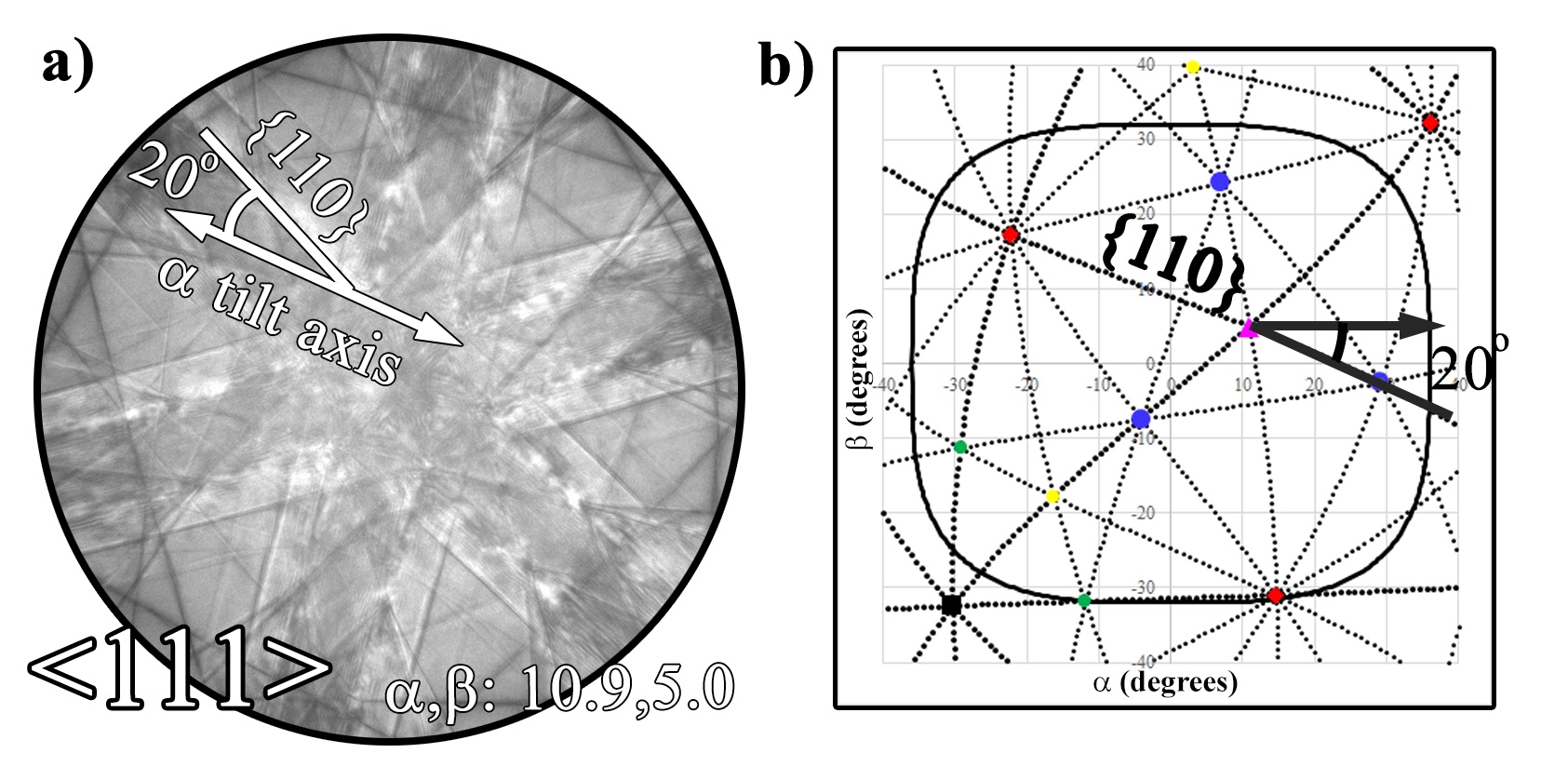
Figure 4.5:Determination of orientation of a known cubic crystal by measuring angles with relationship to the α tilt axis using a Kikuchi pattern (a) and plotting out the pattern with respect to the α tilt axis (b).
4.4Grain Boundary Characterization
The notion of crystals as physical objects using vectors was considered in the development of the mathematics for orientating crystalline material with the double tilt stage to more logically tie it to the sample as a physical object. Microstructural analysis is highly dependent upon objects that, while being often crystallographically related, are not themselves crystalline. Objects such as grain boundaries, surfaces, and interfaces are all important to microscopic analysis, and as such, the description of their motion is of great interest to microscopists. In Practical Derivations, an interface calculator was derived which allows full control of finding a boundary on edge, and how to tilt along the long axis of the boundary. This is discussed through a variety of different techniques in these papers, and there are limitless protocols for which having this control could be utilized.
One example of how this enables nanocartography is through the analysis of nanocrystalline phases on a grain boundary. The difficulty of nanocrystalline phase identification is often related to the size limitation of selected area diffraction apertures. Once an aperture becomes too small, it can start to influence the scattering of the probe, thereby skewing the crystallographic information within the sample Thomas, 1962Carter et al., 1996. With advanced instrumentation, nanobeam analysis techniques were developed to overcome this limitation, but they themselves suffer from being too site specific. That is to say, in nanobeam mode it becomes difficult to position the site-specific region with respect to the rest of the sample given that the beam width is on the order to 10-50 nm. An appropriate analogy is the use of the Ronchigram to align aberration probe corrected beams because they are on the order of a fraction of an angstrom (and hence cannot be observed on a physical detector). Having full control and knowledge of not only the crystalline components of the sample but as well, the control over orientation of interfaces can serve to overcome much of these limitations.
Most often nanocrystalline phases on interfaces and boundaries are crystallographically oriented to one of the adjacent crystalline phases, and therefore knowing the orientation of the adjacent matrix will make phase identification of the nanocrystalline phases more accessible Bhadeshia, 1987. Yet, if the interface is not oriented correctly (i.e., not viewed edge on), parasitic reflections from an adjacent grain could skew identification. Therefore, a protocol could be utilized by which to first solve the crystal orientations of both crystals (Figure 4.6), and then subsequently find the interface on edge condition. In Figure 4.6 (with the sample at α,β:0,0) the grain boundary is observed ~10° from an edge on condition and 38° to the α tilt axis. By overlaying the directions of the interface lines over top of the crystalline solutions, a map of the optimum orientation for crystallographic analysis could be achieved. There will be only one tip/tilt position on the tilt directions normal to the interface where the boundary would be oriented edge on (in this condition 10° from α,β:0,0 is α,β:-6.1,-7.9), and once at that orientation the boundary could then be tilted along the its long axis to keep the boundary edge on (along the blue line). By tilting along the boundary in the edge on condition to a position where either adjacent grain is near a low index pole/ZA, selected area diffraction (SAD) could then be achieved without parasitic reflections from either adjacent grain (e.g., G1 oriented to [121] at α,β:17.4,-26.8, with no major pole present in G2). Any systematic reflections (albeit weak due to the small volume of material) could then be compared against the low index orientation of either grain, and additionally since the orientation of the opposite grain would already be known, any reflections from that grain could easily be identified and temporarily ignored. Additionally, if a tilt condition exists where both grains are preferentially oriented (e.g., α,β:-28.8, 11.9 where G1 is oriented to the [12-1] and G2 is on the [110]) when the grain boundary is edge on, HAADF atomic column imaging can clearly elucidate the boundary conditions.
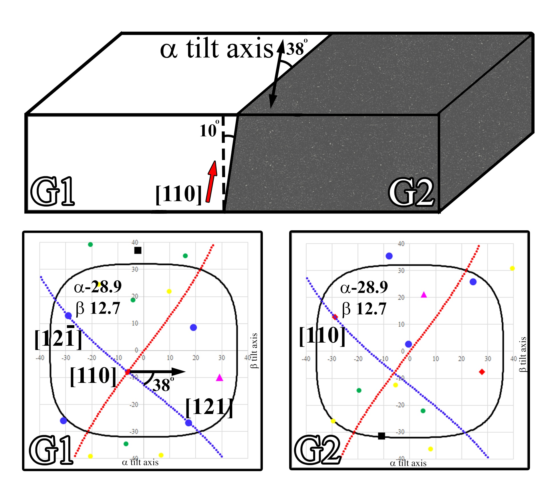
Figure 4.6:Schematics illustrating a protocol for determining the grain boundary physical orientation relationship to the adjacent crystalline grains. At α,β:0,0 the boundary is ~10° from an edge on condition with the boundary oriented 38° from the α tilt axis. The crystallographic solution for both grains is presented with an overlay of the tilt orientations for tilting the boundary along (blue) and against (red) the long axis of the boundary.
4.5Multiple Session Sample Analysis
While the impetus for developing nanocartography as a technique was to rapidly and accurately perform tiling along known planes and between known poles/ZA (similar to the impetus for the development of ALPHABETA Cautaerts et al., 2018), it soon became more evident as to the real power behind utilizing vector calculations. While any number of publications have outlined the geometry and mathematics to navigate a double tilt stage as well as various crystals, none have taken into consideration the ability to re-orient the sample for additional analyses. Through the inclusion of the rotation matrix, which utilizes improper rotations as reflections, sample analysis can be done over multiple sessions on one microscope without losing the previously mapped crystallographic or interface positioning. As previously mentioned, this opens the ability to take full advantage of smaller and smaller analysis windows in an era where crowd sourcing of the instrument places microscope time at a premium.
More importantly, with the ability to map out samples it makes collaborations between institutions more attractive. Figure 4.7 illustrates how this might work between an institution such as Colorado School of Mines (CSM) and Pacific Northwest National Laboratory (PNNL). Regardless of what peripherals, detectors, or systems are on a single microscope, the ability to measure the α tilt axis on a double tilt stage, provides a manner to communicate the data collected from one scope to another. The provided movie illustrates how diffraction patterns would rotate with sample rotation in the cradle.
At CSM a sample could be loaded and two fiduciary markers would be logged. The first, a global fiduciary marker in relation to the holder (which will later be accounted for in the rotation matrix as and ). Once loaded, a conspicuous local fiduciary marker on the sample itself is also measured. Mapping of any of the crystals on the sample surface could be performed, with each pole/ZA being logged. The sample and sample map could subsequently be shipped to PNNL for further analysis. This could be done for any reason; lack of a specific technique, higher end instrumentation, or collaborative analysis. This could save a great deal of time, money, and effort in requiring staff from each institution to travel.
At PNNL, regardless of reason, the sample could be loaded in a horizontally flipped orientation. The reason for a change in orientation could vary from a simple mistake to a geometric necessity (e.g., a double tilt holder which can only load the sample with the crescent normal to the long axis of the stage to account for the position of XEDS detectors), but because the mathematics derived in this work, this can be taken into account and the original crystallographic data can be translated. The identical fiduciary marker initially recorded is measured along with the horizontal flip of the sample, and the conversion of the previously noted poles/ZA are quickly achieved. The movie included in Figure 4.7 demonstrates how diffraction patterns would rotate commensurate with sample rotation in the cradle.
- Olszta, M., Hopkins, D., Fiedler, K. R., Oostrom, M., Akers, S., & Spurgeon, S. R. (2022). An Automated Scanning Transmission Electron Microscope Guided by Sparse Data Analytics. Microscopy and Microanalysis, 28(5), 1611–1621. 10.1017/S1431927622012065
- Xie, R.-X., & Zhang, W.-Z. (2020). [tau]ompas: a free and integrated tool for online crystallographic analysis in transmission electron microscopy. Journal of Applied Crystallography, 53. https://doi.org/10.1107/s1600576720000801
- Zhu, Y., Ophus, C., Toloczko, M. B., & Edwards, D. J. (2018). Towards bend-contour-free dislocation imaging via diffraction contrast STEM. Ultramicroscopy, 193, 12–23. https://doi.org/10.1016/j.ultramic.2018.06.001
- Phillips, P. J., Brandes, M. C., Mills, M. J., & De Graef, M. (2011). Diffraction contrast STEM of dislocations: Imaging and simulations. Ultramicroscopy, 111, 1483–1487. https://doi.org/10.1016/j.ultramic.2011.07.001
- Sun, C., Müller, E., Meffert, M., & Gerthsen, D. (2019). Analysis of crystal defects by scanning transmission electron microscopy (STEM) in a modern scanning electron microscope. Advanced Structural and Chemical Imaging, 5, 1. https://doi.org/10.1186/s40679-019-0065-1
- Thomas, G. (1962). Transmission electron microscopy of metals. Wiley. https://doi.org/10.1107/S0365110X6200287X
- Carter, B., Carter, D., & Williams, D. (1996). Transmission Electron Microscopy: A Textbook for Materials Science. Diffraction. II. Springer. https://doi.org/10.1007/978-0-387-76501-3
- Bhadeshia, H. (1987). Worked examples in the geometry of crystals. Institute of Metals. https://doi.org/10.1107/S0108767301006882
- Cautaerts, N., Delville, R., & Schryvers, D. (2018). ALPHABETA: a dedicated open‐source tool for calculating TEM stage tilt angles. Journal of Microscopy, 273. https://doi.org/10.1111/JMI.12774

