Nanocartography: Planning for success in analytical electron microscopy
Practical Derivations of Nanocartography
The methodologies and protocols derived subsequently in this paper build off the derivations in Naviation and Orientation, and serve to better interface crystallographic and stage motion in a practical manner. Transmission and scanning transmission electron microscopy (S/TEM) data presented in this paper were collected on an aberration, Cs corrected JEOL ARM200CF and include diffraction, convergent beam electron diffraction (CBED), bright field (BF), and STEM high angle annular darkfield (HAADF). The data are generic examples used for demonstration purposes to elucidate various protocols and will not be described further than identification of the imaging mode and/or base crystal type.
3.1K-space Calibration, Small Angle Tilting
In the pursuit of analyzing beam sensitive samples or smaller volumes within a polycrystalline field it is often necessary to have a guide by which to be able to blindly drive the stage while either blanking the beam, lowering the magnification, or defocusing the beam (in STEM) such that the area of interest is not accumulating dose or is lost amongst a field of other adjacent crystals. The approaches provided in later sections presupposes that one has some knowledge of the crystal, but often if the sample is only tilted some observable distance from a desired ZA or plane of atoms, it is not necessary to understand the overall orientation, just that a specific ZA is within a small tilting angle. Therefore, once the location of the α and β axes have been identified, it is conceivable to create a small angle tilt template such that if a sample is, for example, less than 5˚ off a ZA, one can rapidly calculate the tilt coordinates without further observation of the sample past the initial collection of the current pattern.
This is important for beam sensitive samples and small samples within a polycrystalline matrix, where either the beam can destroy the sample or the non-eucentricity of the stage translates the sample away from the field of view during tilting. In order to calibrate a tilt map, one of two methodologies can be utilized depending on level of programing expertise (for example in Gatan Microscopy Suite).
Calibration of the digital capture of k-space is first necessary such that a subsequent point and click on the computer screen to tilt any desired pole/plane to the center position could be accomplished (Figure 3.1). At any point within the double tilt stage the immediate motion of the stage traverses in a linear fashion out to ~7-10°. At this point, due to the motion of the β tilt in relation to the α, any trace begins to rotate and nonlinear effects become noticeable. Since most local digital fields of view illuminate ~5-6° of tilt (~90-100 mrad), the calibration will be considered linear. Only the α need be considered, as the entire relationship of tip/tilt map can be deduced from this measurement.
The calibration of the α tilt is required for the specific TEM approach and should be performed with a crystalline sample with a ZA fiduciary marker close to α,β: 0,0. The location of the probe (red dot/circle in Figure 3.1) or transmitted beam should first be identified digitally (i.e., the pixel location on the screen, x/y, should be correlated with the center of the beam) and noted as the origin (x0,y0). Next, the crystal can be tilted in the pure negative or positive α direction ~4-5° (or to the edge of the field of view) such that the digital position (xref,yref) can be calibrated to the tilt (green dot/circle in Figure 3.1). This position will be denoted as the calibration, and a calibration vector can be produced by subtracting the reference position from the origin. This vector, shown in Eq. (3.1), is normalized to produce a unit vector in the direction of α tilt. The direction of β tilt is perpendicular to this, and the unit vector is shown in Eq. (3.2).
The tip/tilt coordinates for any position (x,y) in the field of view (blue dot/circle in Figure 3.1) can be calculated to align the feature of interest (e.g., zone axis) with the probe by decomposing this location into components along and . The decomposition must be solved for the amount along () and the amount along () in Eq. (3.3).
Solving this system of equations for the weights yields:
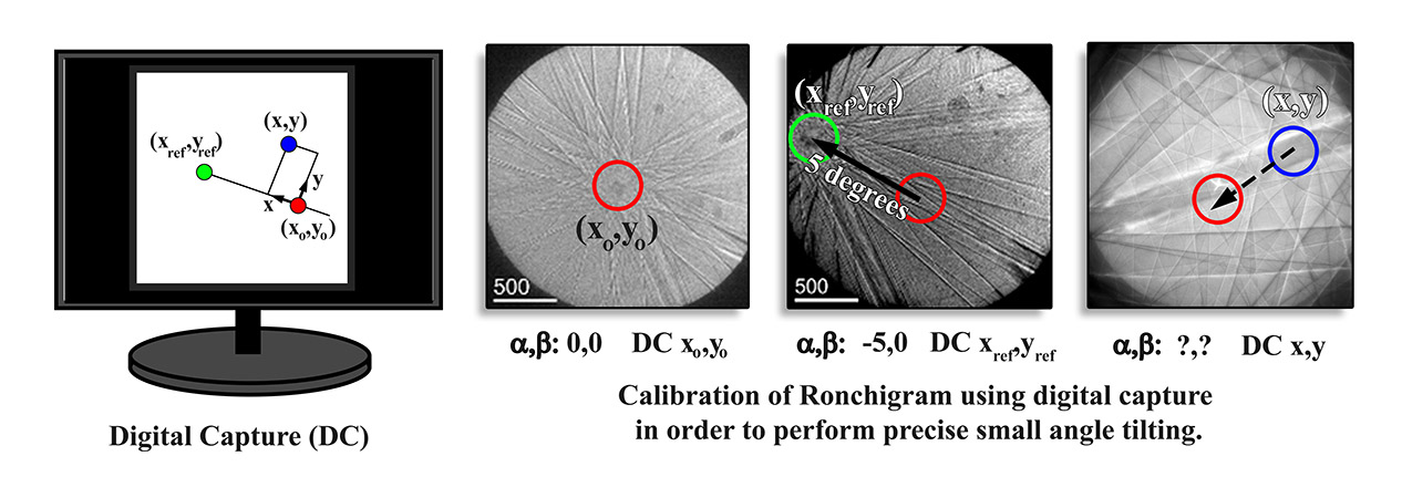
Figure 3.1:Calibration of digital capture for precise, small angle sample tilting.
Once the weights are known, they are converted to tip/tilt coordinates using a scaling factor that was derived from the initial α calibration tilt divided by the length of the vector. The equation for scaling factor is:
Utilization of these formulae allows for precise small angle tilting using CBED or a Ronchigram where there could be a high density of additional Kikuchi lines from adjacent, smaller crystals. More importantly, if the sample is beam sensitive only a single image capture need be collected to predict how to tilt within the field of view in k-space.
3.2Center-beam Darkfield Tilting
Precise off axis tilting of the electron probe using the condenser lens deflector coil system has long been utilized to examine the location of specific diffracted beams (center beam darkfield Carter et al., 1996), to perform techniques such as hollow cone diffraction Kondo et al., 1984, and conduct precession electron diffraction (PED) Vincent & Midgley, 1994Midgley & Eggeman, 2015. Tilting the beam can be considered a conjugate of tilting the sample, and hence the use of digital capture can be utilized to dictate the tilt of the beam.
If the same mathematical calculations are completed with the tilt conditions replaced with condenser lens deflector outputs, the precise beam deflections can be utilized (Eqns. 3.1-3.6). The difference is that the beam deflections are most often read as hexadecimal, and therefore the calculations need to utilize the hexadecimal outputs instead of stage tilt positions.
This technique can be utilized in a wide variety of methods to examine darkfield tilting and is important for analysis of beam sensitive samples. Once a single diffraction pattern is collected, the beam can be blanked by appropriate methods, and the beam tilt conditions can be performed by pointing and clicking on the viewing screen to obtain the correct deflections (e.g., Figure 3.2a where the (-1-31) spot is deflected to the central beam). Similarly, when there is no visible diffraction spot but there is a crystalline phase suspected (or possibly a weak superlattice reflection), digital alignment can be performed blindly (white circle in Figure 3.2a). Additionally, the beam could be deflected in a circular manner by which to explore all possible g-vectors in k-space during a long, darkfield exposure (Figure 3.2b). This technique could then be utilized to program in all desired g-vectors of a given crystal system at once and compare the resulting image to a second set of deflections corresponding to a different crystal (e.g., FCC versus BCC). It is beyond the scope of this paper to go into more detail, but precise digital control of the beam deflectors in TEM mode could be highly beneficial for a wide range of materials analyses.
![Example of digital capture darkfield tilting using a
diffraction pattern of an FCC crystal in the [211] orientation (a),
and a schematic illustrating a theoretical example of deflecting the
probe in a circular manner (b).](https://pub.curvenote.com/01919ca9-b718-74ab-9b96-74b341835a99/public/Figure 13-27b2b91ebe0f81f25f9fc90bcfef6f25.jpg)
Figure 3.2:Example of digital capture darkfield tilting using a diffraction pattern of an FCC crystal in the [211] orientation (a), and a schematic illustrating a theoretical example of deflecting the probe in a circular manner (b).
3.3Image Montaging
Although not directly related to the stage tilt movement, an additional protocol that has proven extremely productive in scanning electron microscopy (SEM) is the notion of montaging images at a specific magnification/resolution to create a larger image. The increased resolution of the higher magnification maps provides for richer, more meaningful data sets as compared to a single, low magnification overview image. Although in principle an increased resolution could be used at lower magnifications, there is a physical limit to the camera/detector size that makes it prohibitive. Most often on the TEM montaging is performed manually by the microscopist because a small number of maps are required to cover an area of interest, and as well because of the time prohibitive nature of limited scope availability. The ability to automatically montage data has not been a necessary feature on most microscopes, but with the coming age of automation Spurgeon et al., 2020Olszta et al., 2022, there will be a need to perform overnight montaging of samples for data triaging in subsequent sessions. As has been demonstrated throughout this work, the ability to have a map or specific list of commands provides a sense of direction for the microscopist. While a montage could be done manually, gauging where the previous region of interest overlaps with the current image, a table of stage positions would be more beneficial to the user. Given a desired distance, X, image dimension, Y, and necessary image overlap (p, as a fraction) the number of maps necessary to create a montaged image is given in Eq. (3.7). The table of stage positions can then be calculated through Eq. (3.8) where the addition or subtraction of the (X-Xp) or (Y-Yp) terms are a function of the numbering logic of the stage and are added to the previous image coordinates (movie showing montaging in Figure 3.3). This of course takes into account the fact that the sample is flat, and a Z term has not been introduced. This could be addressed for highly titled samples by observing the height at either end of the desired montage range and scaling each position accordingly. This also does not consider the movement of backlash within the stage, and is only meant as a starting point for creating montaged images.
3.4Pure Tilt Between Tip/Tilt Conditions
It is often necessary to calculate the angle between specific tip/tilt conditions, as will be demonstrated later when solving unknown crystal structures. The derivation for computing the angle between stage tilt coordinates (α,β) is based off of the tip/tilt convention, where the stage tilt is first rotated about the α tilt axis Eq. (3.9) and then subsequently about the β tilt axis Eq. (3.10) to the to the beam normal [001] Eq. (3.11). That is, given a vector at the [001] position it can be rotated to any tip/tilt position (α,β) via Eq. (3.12).
This rotation can be performed for any two sets of tilt conditions, and , and therefore the dot product between two vectors Eq. (3.13) will provide the angle between the two tip/tilt conditions Eq. (3.14). It should be again be noted that the order of rotation, α then β, is important, and reversal of the order will provide erroneous results.
3.5Grain Boundary Misorientation
Possessing the crystallographic solution for two adjacent crystals (Figure 3.4a and Figure 3.4b) of the same crystal system provides additional information, namely the grain boundary misorientation angle and axis of rotation Chesser et al., 2020. This ability to calculate and report this additional sample descriptor can be a powerful tool where the only additional analysis that must be performed is the calculation (i.e., only the two crystal orientations are necessary). There are a number of methods by which to derive the local misorientation Jeong et al., 2010Liu, 1994Liu, 1995, but in all cases the crystal orientation of two adjacent crystals are utilized to determine the directions of the unit vectors (Figure 3.4c). The comparison of the unit vectors of each crystal are used to calculate the misorientation angle about a shared misorientation axis ([uvw]) through a misorientation matrix (Figure 3.4c). The first step in developing this matrix is to solve for the location of each of the unit vectors in each crystal.
In Figure 3.4, Crystals A (a) and B (b) are observed in a given orientation, and the given tip/tilt positions of any three vectors within each can be determined through the crystallographic solution (e.g., Crystal A [110], [111] and [201], and Crystal B [110], [112], and [111]). Note that the choice of these three is arbitrary, but that they must be linearly independent and contain three distinct directions (i.e., [111] and [222] would not be distinct directions). These three vectors can be used to determine the location of their respective unit vectors (Figure 3.4d).
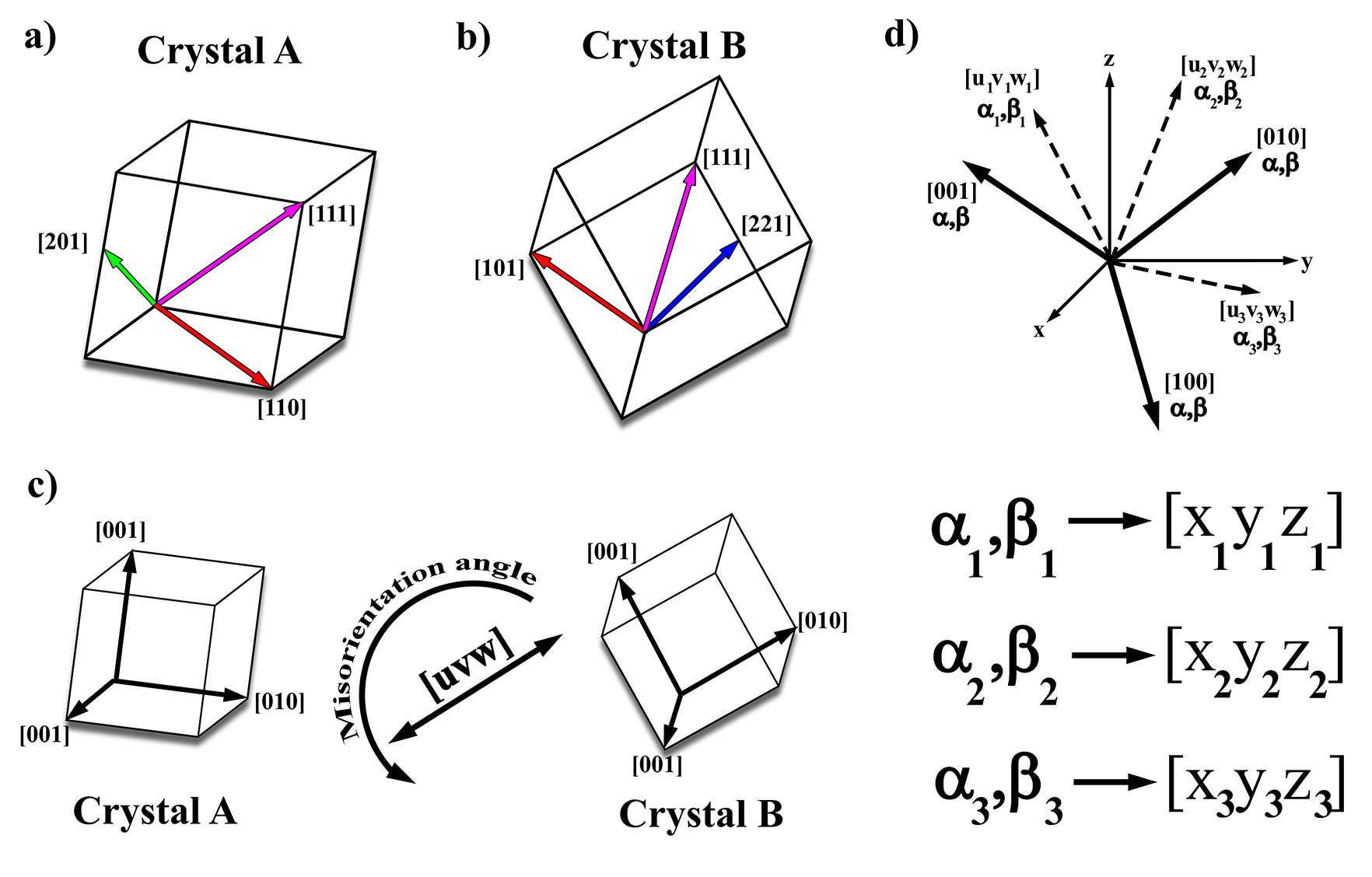
Figure 3.4:Schematic illustrating how the local misorientation between two crystals is formulated. a) and b) Crystals A and B in a given orientation, respectively. c) Misorientation angle and axis between the two crystals. d) Conversion to primary axes coordinate system.
The development of a misorientation matrix will describe the pure angle required to rotate the unit vectors of Crystal A to align with the unit vectors of Crystal B (Figure 3.4c) and the shared axis between the two crystals about which this rotation can be accomplished. In Cartesian space the orientation of the vectors can be utilized in developing this matrix, but in the microscope the description of the vectors are defined by the coordinates of the double tilt stage.
The three observed or known vectors for one crystal (e.g., [uA1,vA1,wA1]) are observed at a given tip/tilt position (e.g., αA1,βA1) (Figure 3.4d). These tip/tilt positions need to be converted into Cartesian space similar to the operation performed in Eqns. 3.9-3.14 during the development of the angle between tilt positions (e.g., [xA1,yA1,zA1]). In order to derive the Cartesian vector form of the unit vectors ([100], [010], [001]) for the crystal, the tilt position vector in Cartesian form ([xA1,yA1,zA1]) is first required to have the same magnitude as the crystallographic vectors ([uA1,vA1,wA1]). This can be accomplished by multiplying the tilt vector by the length of the crystallographic vector Eq. (3.15).
Similar expressions for the other two poles can be calculated, where the subscript 1 has been replaced with either 2 or 3. It is necessary to find three Cartesian vectors which add up to the three known vectors given the linear combination weights determined by the crystallographic poles.
These three unknown Cartesian vectors are the unit vectors that describe the orientation of the crystal. In the microscope, regardless of the sample orientation (e.g., [111] at α,β:5,10) the location of the unit vectors (i.e., [001],[010] and [100]) are calculated. These vectors are subsequently utilized to describe how to translate from one crystal orientation to another (e.g., [100] of Crystal A to [100] of Crystal B). The linear combinations that connect these sets of vectors are:
These equations can be solved for the components of the vectors , and since there nine equations and nine unknowns. The details of how these equations are rearranged are in the Appendix, but after gathering like terms, it is equivalent to the augmented matrix:
After row reducing this augmented matrix to reduced row echelon form:
The right-hand side of the row reduced matrix produces the elements of the vectors , and that give the axes of the crystal in Cartesian vector form. The reason these three vectors are necessary is because they give the rotation matrix that describes the orientation of the crystal from the standard orientation where the crystallographic axes ([100], [010], [001]) align with the coordinate axes (). This standard orientation alignment is the common feature that connects any crystal orientation to another. The rotation matrix is found from the transpose of the right-hand side of the row reduced augmented matrix. This can also be described as the unit vector matrix in that it can be used to describe the location of the unit vectors for a specific crystal.
The previous rotation matrix was derived for Crystal A , but the exact procedure applies to Crystal B without any modifications beyond the subscript, and is denoted by:
Both of these rotation matrices convert from the standard orientation to the current rotation of their respective crystal. To get from one orientation to the other requires going from the current orientation back to the standard orientation and then to other crystal orientation. Mathematically, this is done by using the inverse of the rotation matrix to get back to the standard orientation.
These two overall rotation matrices are the misorientation matrices that describe the relative orientation of one crystal to another. Most frequently, the desired information is how far apart two crystals are misaligned and about which axis they must be rotated so that they would become aligned. This is called the axis-angle representation of the rotation matrix. If the general form a misorientation matrix is:
Then the axis-angle representation is, where θM is the misorientation angle and is the misorientation axis:
It should be noted that the relative orientation solution for the adjacent crystals is important in the calculation of the misorientation angles, depending on the crystal system chosen. This is especially true for higher symmetry systems (e.g., cubic) where redundant vector normals allow accurate prediction of tilting from one pole to another, but the relative orientations will become important when performing mathematical calculations such as the misorientation angle. It is beyond the scope of this paper to include a full discussion of all of the possible symmetrical operators, but the reader must be aware of this when utilizing stage tilts in the TEM to perform these calculations.
Lastly, in order to complete the full description of the grain boundary, the interface must be further characterized to describe the orientation of the plane of atoms with respect to the boundary and the adjacent grain. To access this data, the physical orientation of the grain boundary as a physical plane with respect to the stage is required. Once the tip/tilt conditions are determined, then these coordinates can be used to calculate the description of the plane normals.
3.6Interface/Boundary Tilting
The ability to correctly and accurately predict the motion of crystals in an electron microscope using a double tilt stage is crucial to collecting the optimal data over a wide range of fields of study. In Navigation and Orientation, a full explanation of how to derive these calculations was conducted; first the crystal was treated as a physical object and then subsequently a physics based filter was applied through the structure factor. The advantage of this approach is that the motion of non-crystalline samples can be treated in the same way as the derivation of directions for planes or tilts between poles as interfaces are physical planes. Therefore, the ability to identify the orientation of the long axis with respect to the α tilt axis can be predicted similar to identifying the orientation of a plane of atoms.
As will be demonstrated in subsequent sections, this can be further utilized in a variety of techniques from creating oblique tilt series to rapid analysis of grain boundaries edge on. More importantly, prediction of the interface movement allows for more accurate data collection as it can also be related to adjacent crystalline material. For instance, if an edge on boundary condition is determined, then the boundary can be subsequently tilted along its long axis to any tilt condition that may be favorable to the adjacent crystal, such as a pole or specific plane of atoms. Additionally, when the interface is edge on, the adjacent crystallographic normal(s) can be calculated if the crystallographic solution of the crystal(s) has been measured.
The approach for predicting interface motion is similar to that of calculating planes of atoms, except that for planes of atoms there is an explicit normal previously defined by the plane of atoms in question. For an interface, the starting tip/tilt conditions are the only information available (e.g., α,β:-5,10 in Figure 3.5) as well as the measure of the long axis to the α tilt axis (e.g., θ in Figure 3.5 of which the grain boundary is measured at ~75°). Note that the sign of rotation of the boundary to the α tilt axis is reversed between Figure 3.5a and b because of the sign convention of how the α tilt axis is calibrated. The relationship of the current tilt conditions to the fiduciary angle to the α axis is important because, as was demonstrated in Navigation and Orienation for planes of atoms, in the double tilt stage linear features will rotate when tilted to higher angles. That is to say, θ in Figure 3.5a will vary slightly based on the given α,β tilt conditions.
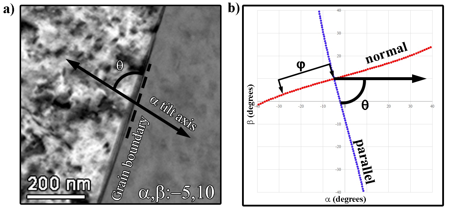
Figure 3.5:Plotting tip/tilt coordinates for interface analysis. A TEM (BF) image of a grain boundary is shown in with the angle to the α tilt axis (θ) highlighted (a). The trace of the boundary on a tip/tilt diagram (b) illustrates the angular movement (φ) normal to the boundary conditions shown in (a).
As there is no crystallographic information utilized, the current tilt position (e.g., α,β: -5,10 in Figure 3.5a and b) is required to be converted into a Cartesian vector similar to what was performed in the calculation of the misorientation matrix. In order to calculate the vectors parallel and perpendicular to the direction of the interface Eqs. (3.31) and (3.32) need be derived, respectively. These two vectors lie in the xy plane and are determined solely by the angle θ.
Navigation and Orientation details a rotation about an arbitrary axis (see Appendix), and this will be used to rotate about both the vectors and Eq. (2.18). The general formula for rotation of angle φ about an axis of rotation (with length equal to one) is:
In the case where is the axis of rotation, the tilt series is perpendicular to the interface. Conversely, in the case where is the axis of rotation, the tilt series is parallel to the interface. In either case, the angle of rotation (φ) determines how many steps will be in the tilt series (Figure 3.5b). Typically for a full rotation , hence there will be 360 steps in the series before returning to the original orientation. The simplified rotation matrices are:
As with all other tip/tilt conversions, the Cartesian vectors calculated in Eqs. (3.34) and (3.35) need to be converted to tilts through Eqs. (3.36) and (3.37) (note these are functionally the same as Eqns. 2.23 and 2.24). These derivations will subsequently be utilized to create oblique tilt series and perform precise interface orientation calculations.
3.7Calculating Interface Orientations/Rapid Grain Boundary Analysis
Before the advent of atom probe tomography (APT), TEM had long been the most advanced technique for understanding materials properties at the highest chemical resolution Blavette et al., 1993Carter et al., 1996. Even with the ability to more precisely analyze interface chemistry by APT, S/TEM still provides a manner by which to analyze chemistry in addition to relating it to crystallography and other microstructural features such as dislocations and defects. More importantly, whereas the region of interest in APT is highly localized and is dependent on precise sample preparation (e.g., it is possible that only a small portion of an interface is captured within one tip), S/TEM allows a more global perspective for any given sample. One sample may contain tens of grain boundaries with lengths on the order of micrometers, thereby allowing the user to probe and provide a more representative analysis of the microstructure and microchemistry.
The ability to harness this much information for any given microstructure/sample is predicated on the speed of analysis combined with the correct orientation. In terms of interfaces, it is absolutely necessary that a boundary be analyzed edge on in order to best assess chemical gradients. For example, the depletion in sensitized stainless steels due to irradiation can be measured Simonen & Bruemmer, 1998 and subsequently used to model the behavior of a material as a result of various external stimuli (e.g., heating, irradiation, chemical diffusion). Therefore, rapid and accurate alignment of interfaces on edge (i.e., completely aligned with the electron beam direction) is tantamount to performing the best possible analysis.
The utilization of a double tilt stage makes this entirely possible based on a number of tilting techniques. First, each tilt axis can be rocked independently in a positive and negative manner while the width of the desired interface is minimized. This requires that the same interface region be kept in the field of view during each tilting step. If the boundary has any deviation along its long axis (e.g., grain boundary curvature), determination of exactly when the boundary width is minimized can be challenging. Even more difficult is the assessment of the width of the boundary during tilting of the non-eucentric tilt axis (β), as the sample location often drifts even in piezo controlled stages. More importantly, as the length scale of the boundaries decreases towards the sub micrometer level, tracking the exact position of the boundary can be tedious and time consuming even on the eucentric tilt axis (α). In order to minimize the difficulty of tilting on the non-eucentric axis, a second method that can be employed is to measure the rotation of the long axis of the interface to the α tilt axis, remove the sample from the microscope, and then physically rotate the sample to such that it can be tilted solely on the eucentric axis (i.e., the long axis of the boundary is physically aligned along the non-eucentric axis so it can be tilted against the interface). The problem with this method is the amount of time for each analysis and lack of fidelity in physically rotating the sample. There do exist double tilt rotate holders specifically for this type of alignment, but they are most often not optimized for chemical analysis and are typically not standard to most microscopes.
Using the tilt methodologies developed in previously, a grain boundary in any orientation can be tilted on edge by collecting two tilt conditions where an interface width is measured at each tilt condition (provided reasonable assumptions of sample thickness and tilt range of a given holder). When the boundary is tilted against its long axis in a purely orthogonal manner in a known quantity (φ in Figure 3.5b), the geometry of an inclined sample can be measured to determine not only the necessary tilt conditions to be aligned on edge, but as well provide a reasonable measure of the sample thickness (Figure 3.6).
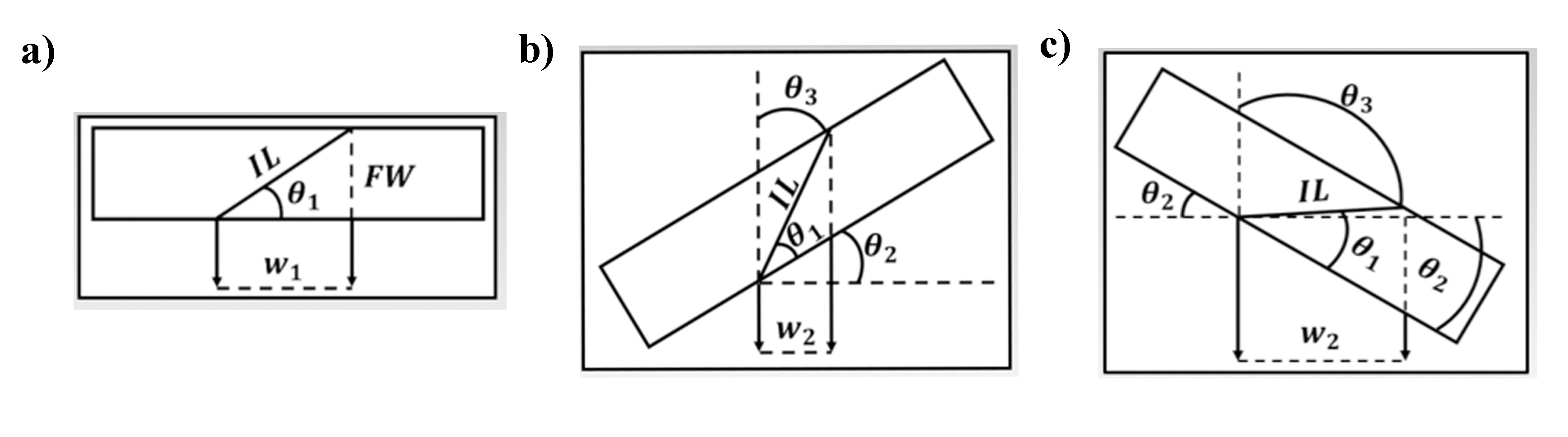
Figure 3.6:Schematics illustrating calculation of interface on edge conditions and sample thickness. a) Sample in original tilt, b) sample tilted negatively, and c) sample tilted positively.
For any given interface, the projected width (Figure 3.6a, w1) can be measured at the current tip/tilt conditions through the difference in contrast where the interface intersects the top and bottom of the foil. While initially unknown, the interface has an inclination angle to the foil normal (Figure 3.6, θ1). The projected width (w1) can be related to the interface length (IL) by the cosine of the inclination angle (θ1, Eq. (3.38)), and the foil width (FW) can be calculated by the sine of the inclination angle Eq. (3.39). Additionally, while the directionality of the boundary (top left to bottom right, or top right to bottom left) is inherently unknown, the manner in which the calculations are performed makes this orientation irrelevant.
The angle of the interface’s long axis to the α axis can be measured (i.e., θ in Figure 3.5a) and using Eqns. 3.31-3.37, the tilt conditions for a pure orthogonal tilt normal to the boundary can be calculated (Figure 3.6b and c, θ2). This angle is commensurate with φ in Figure 3.5b, and these tilt conditions can be either positive or negative (Figure 3.6b and c) based on the stage reference. For example, at a starting condition of α,β:0,0 with the boundary at 45° to the α axis and a tilt of 10° (θ2 or φ) puts the tilt stage at (α,β:-7.1, -7.1) or (α,β:7.1, 7.1).
At this tip/tilt condition, a second apparent grain boundary width (w2) can be measured (Figure 3.6b). Depending on magnitude of w2 as compared to w1, and knowing the foil width (FW), Eqs. (3.39)-(3.41) can be used to calculate the angle necessary to tilt the boundary edge on, θ3, of which can be derived in the following manner.
Once tilted, the projected width of the boundary (w2) can be related to the angle necessary to tilt the interface on edge (θ3) using trigonometry.
The interface length (IL) is initially unknown, but is constant between tilts and can be found using the Pythagorean Theorem once the initial width (w1) and the foil width (FW) are known.
Substituting this above yields the final equation for :
In a double tilt stage the trace of a plane (or boundary in this instance) physically rotates due to the S-curve, and therefore there are two manners in which to calculate the final tilt conditions where the interface will be oriented edge on. These calculations consider the measure of the long axis of the boundary to the α tilt axis (θ in Figure 3.5), and this angle will change depending on the current tip/tilt conditions (i.e., in Figure 3.5 θ at α,β:0,0 is 75°, but at α,β:-10,30 it would be change by ~2° due to the S-curve). Therefore, when performing the final tip/tilt calculations the choice of the appropriate measure of θ is imperative. One can either re-measure the angle of the boundary to the α tilt axis at the second tip/tilt conditions, or utilize the starting tilt conditions (where w1 was measured) and the measure of the initial interface angle to the α tilt axis. The pure tilt (whether θ3 or the difference between θ2 and θ3) will depend on which conditions is chosen. Regardless, either can be performed by using Eqs. (3.38)-(3.41) to tilt the sample in a positive or negative fashion by θ3.
This can be visually demonstrated in Figure 3.7a where a theoretical grain boundary measured at 45° to the α tilt axis at starting tilts α,β:0,0 is measured at 40 nm wide. A positive tilt of 25° moves the stage to α,β:17.4,18.3 (along the black dotted line in Figure 3.7a) where the boundary is measured to be 60 nm wide (an increase of 20 nm), meaning the boundary needs to be tilted -35.4° from the starting tilt conditions (α,β:0,0) to a final tilt condition of α,β:-24.2,-26.7. Under these conditions, the sample thickness would be ~56 nm thick. If the final, edge on, tilt calculations were performed from the second tilt condition (α,β:17.4,18.3, red dotted line in Figure 3.7a) without re-measuring the grain boundary angle to the α tilt axis (which has rotated by ~2.5°) the final tilt conditions would be (α,β:-26.1,25.0) which is ~2.4° from the correct position. While still within the precision of most double tilt stages, it would not be correct.
The initial input tilt (Figure 3.6, θ2) will be dictated by the initial interface width due to the possibility of the tilting the sample through the edge on condition, thereby invalidating the calculations. The wider the initial boundary width, the more the initial tilt can be applied. To fully account for the possibility of tilting through the edge on condition, a third tilt and a third width, w3 would be necessary, but by assessing the approximate width of the sample (e.g., ~100 nm) and the initial interface projected width (w1) a protocol can be developed by which to determine the initial normal tilt (θ2).
Figure 3.7b provides a calculated guide for applicable tilt angles provided a starting apparent boundary width (w1) for a number of approximate sample thicknesses as to not invalidate the calculations put forward in Eqns. 3.38-3.41. In the theoretical example shown in Figure 3.7a where the sample was on the order of ~56 nm thick and the starting grain boundary width of 40 nm, from Figure 3.7b the starting tilt of 25° was appropriate. If the assumed starting thickness of the sample was ~100 nm, 25° would not have guaranteed that this tilt would not tilt past the edge on condition.
As illustrated in Figure 3.7b, if the starting apparent interface width is on the order of 10 nm, the boundary is nearly edge on already, and a small angle calculation can be utilized (Eqs. 3.38-3.41). Instead of developing a tilt series, these equations can be utilized for small angles (1-5°) to tilt a boundary or interface normal to its long direction to close the apparent width of the boundary. The utilization of this rapid interface calculation methodology allows for successive, rapid analysis of any number of grain boundaries regardless of orientation to one another. After one boundary has been tilted edge on, an adjacent boundary width can be measured and then tilted edge on.
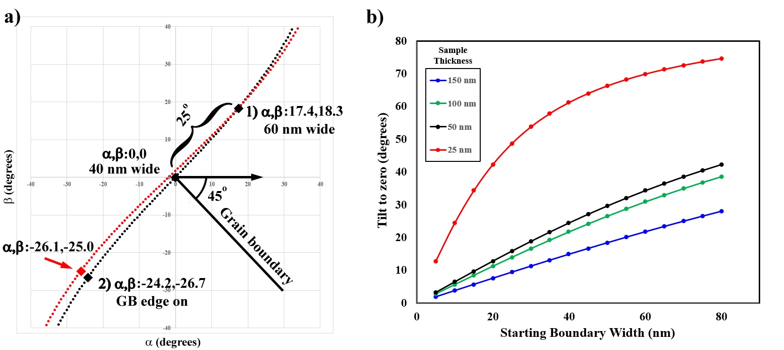
Figure 3.7:Tip/tilt map of a theoretical grain boundary tilted edge on (a), and plot of normal tilt value versus initial projected interface width (w1) for a number of sample thicknesses to gauge the applicable normal tilt angle (θ2) without crossing over the edge on condition (b).
3.8Interface/Crystallographic Normals
Predicting and controlling the motion of crystals and interfaces is important for grain boundary descriptions, determining growth directions of oxides from surfaces, and orientations of facets. In describing the relationship between two crystals, the first step is to determine the misorientation angle and axis (Eqs. (3.29) and (3.30)). This data is commensurate with what is collected in electron backscatter diffraction (EBSD) in SEM, but TEM provides the advantage of further being able to describe the grain boundary orientation, as in Figure 3.8. The inclination of the grain boundary with respect to the stage, as shown in Figure 3.8a for grain 1 (G1), is a known variable and can be solved to orient the grain boundary edge on (Eqs. (3.38)-(3.41)), as shown in Figure 3.8b. Given these tilt conditions, the angle of the grain boundary to the α axis (θ in Figure 3.5a and Figure 3.8b) and the crystallographic solution of the two adjacent crystal(s), the crystallographic normals and planes to the interface can be calculated (solid red arrow in Figure 3.8b).
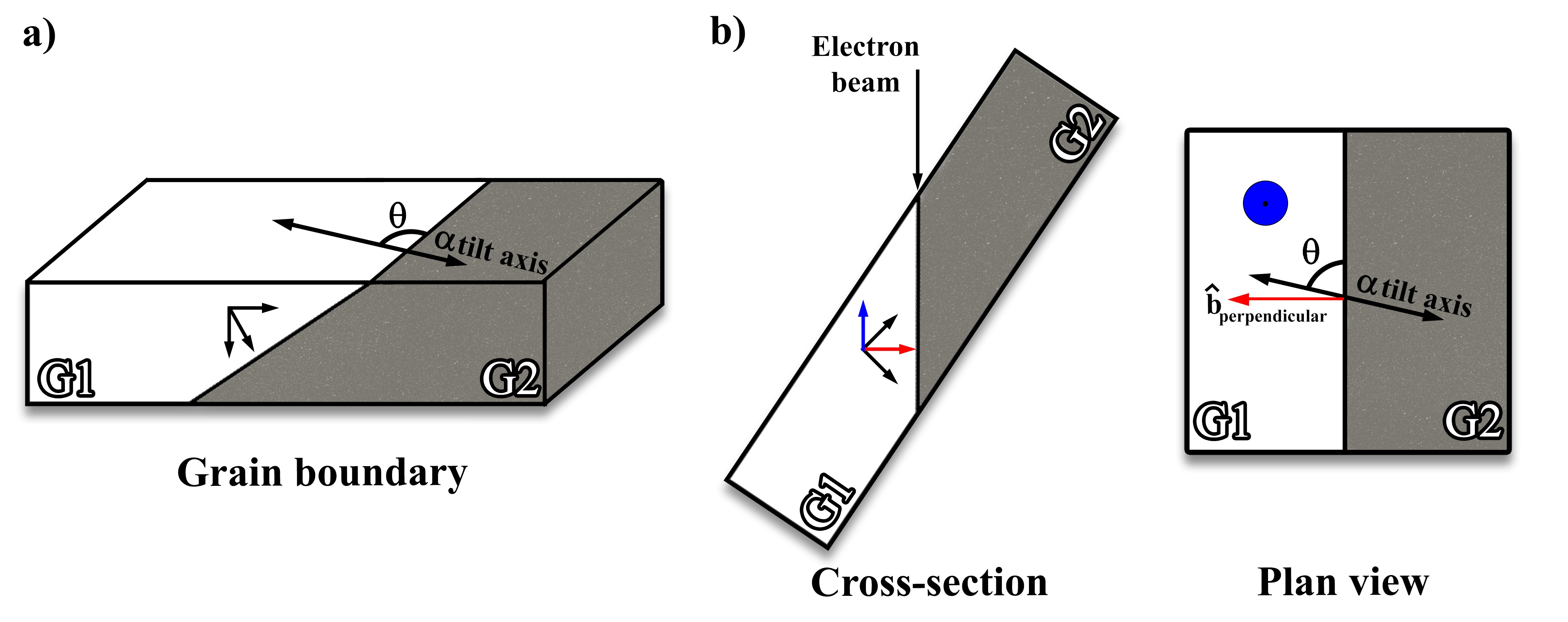
Figure 3.8:Schematic illustrating a grain boundary between two grains (G1 and G2) in a standard orientation (a) and with the boundary oriented edge on to the electron beam (b) shown in both cross-section and plan views.
As has been demonstrated through Eqs. (3.15)-(3.24), provided three known vectors with specific α,β coordinates the unit vectors for the crystal (i.e., [001]) can be derived, and therefore the vector describing any tip/tilt position (α,β coordinates) within that crystal can be described (e.g., the blue arrow/dot in Figure 3.8b for G1 in the edge on condition). This vector can be calculated by multiplying the rotation matrix of the given α,β conditions (Eqs. (3.9) and (3.10)) by the unit vector matrix Eq. (3.24) to form a rotation matrix at that specific α,β tilt condition Eq. (3.42). This in effect rotates the unit vector at that specific tilt condition to the beam direction [001], and as such multiplying the inverse of this matrix by the beam direction will provide the vector at the given tilt conditions Eq. (3.43).
The unit vector matrix, which describes the location of the unit cell axes, can be subsequently utilized to calculate the vector normal orientation of either crystal (red solid arrow in the cross-section view of Figure 3.13b) since the grain boundary plane edge on is commensurate with the crystallographic plane. That is to say, the orientation of the atomic spacings on the repspective crystallogrpahic faces of the grain boudnary can be determined. The vector normal Eq. (3.32) to the long axis can be calculated (dashed line in the plan view of Figure 3.13b) and multiplied by the inverse of the tilt condition matrix, . This vector describes the current tilt conditions where the grain boundary is observed edge on Eq. (3.44). Instead of calculating the vector parallel with the beam direction ([001]) the vector normal is substituted ([-sinθ,cosθ,0], Eq. (3.44)). This can be corroborated using a generic cubic crystal with the [001] positioned at α,β:0,0 and with the [100] oriented along the α tilt axis (such as in Figure 2.7a) and by subsequently inputting any α,β coordinates the listed vector/pole/ZA will be returned (e.g., α,β:24.1,26.6 will be the [112]).
These calculations can be visually corroborated through a tip/tilt map of a basic FCC crystal with the [110] pole plotted at α,β:5,10 (Figure 3.9) with an representative interface observed edge on at α,β:5,10 with the long axis measured 45° to the α tilt axis (blue line). Expansion of the crystallographic tip/tilt plot to ±90° indicates that 90° from the edge on condition (α,β:5,10), the [001] is observed (red circle) at α,β:44.8,-85. Using Eq. (3.14), the angle between (α,β:5,10) and (α,β:44.8,-85) is 90°. If the interface were oriented 135° to the α tilt axis, the [-110] at (α,β:-44.8,-75) would be the vector describing the normal to the interface.
![Plotting of a basic FCC crystal where the
crystallographic solution is provided and the edge on condition is
observed at α,β: 0,0 with the interface long axis 45° to the α tilt axis
(a). The pole normal to the interface is demonstrated to be the [001]
at α,β: 44.8, -85 (b).](https://pub.curvenote.com/01919ca9-b718-74ab-9b96-74b341835a99/public/Figure 20-a7f924119e1b8f5bd9eafcfcfc2ccf71.jpg)
Figure 3.9:Plotting of a basic FCC crystal where the crystallographic solution is provided and the edge on condition is observed at α,β: 0,0 with the interface long axis 45° to the α tilt axis (a). The pole normal to the interface is demonstrated to be the [001] at α,β: 44.8, -85 (b).
The mathematics utilized in these derivations are in the cubic or Cartesian form, and therefore these vectors need to be converted to the native form (for non-cubic systems) through multiplication with the inverse conversion matrix that was derived in the Eqs. (2.1)-(2.3). In order to calculate the plane of atoms in the native form, the reciprocal lattice matrix Eq. (3.45) must be utilized. Note that this is derived from Eqs.(2.28)-(2.31), where Eqs. (2.29)-(2.31) provide the reciprocal unit vectors and Eq. (2.28) is the volume of the cell. The calculation of the native plane of atoms can be derived by multiplying the vector normal Eq. (3.46) by the inverse of the reciprocal lattice matrix Eq. (3.45).
3.9Tilt Series
As previously described, the derivation of tilt motion of interfaces leads to a number of applications in the microscope. Small angle calculations (either normal or parallel with the long axis of the interface) have already been described, and expanding upon these calculations provides a methodology to perform oblique tilt series. While each are simple consequences of the interface motion, a brief discussion of each is necessary to build upon more complex protocols. Electron tomography has matured into a powerful tool for a wide variety of fields, from biology to materials science Hayashida et al., 2019Hayashida & Malac, 2016Lidke & Lidke, 2012. The high tilt requirement often provides limiting factors for this technique including special holders, larger pole pieces, and narrow sample geometries. When performed correctly, tomography can be a useful tool to circumvent the projection issues of TEM, but at the cost of losing the relationship with respect to the rest of the sample. This is considering small, needle shape regions of interest being utilized for tomographic analysis similar to APT analysis.
Tilt series for TEM foils can also be performed along a single orthogonal axis (whether it be α or β) using a double tilt stage, but there are limitations to this approach. Depending on the orientation of objects within the TEM foil, especially when they are oriented obliquely to the stage axes, single axis tilt series may not provide a clear picture. For instance, when a grain boundary decorated with precipitates is tilted in a non-logical manner (i.e., not against its long axis) it is difficult to observe the full distribution of precipitates or voids on the boundary. Yet, when the boundary is tilted against its long axis, the boundary moves in a logical fashion, and the distribution can be readily observed Badwe et al., 2018 (). Equally important, if not more, is the ability to create tilt series along specific planes of atoms that can be beneficial to demonstrate dislocation microstructures in three dimensions Liu & Robertson, 2011Hata et al., 2020Yamasaki et al., 2015.
HBox(children=(Canvas(footer_visible=False, header_visible=False, layout=Layout(width='470px'), resizable=Fals…
Figure 3.10:Tilt series collected across a Ag-Au grain boundary exhibiting void evolution ahead of an stress corrosion cracking (SCC) tip in the binary alloy Badwe et al., 2018.
Using both the interface calculations combined with the crystallographic solution of any grain within the sample allows for rapid collection of tilt series. The tilt series calculations are performed by adjusting the tilt steps in the interface calculation (φ in Figure 3.5b), and most importantly since only small steps are being performed the lack of eucentricity on the β is minimized.
The mathematical derivations (Eqs. (3.31)-(3.37)) for tilting along or against the long axis of an interface at discrete angular steps regardless of orientation (e.g., orthogonal or oblique to the major tilt axes) provides the ability to correctly orient interfaces for spectral analyses, and can also be utilized in combination with the solution of adjacent crystals to create useful tilt series data.
3.10Kikuchi Bands and Diffraction Patterns
The ability to create tip/tilt maps of any crystal system is important for nanocartography at any length scale. Given a known pole and in plane orientation, microscopists can quickly and reproducibly tilt anywhere within the stage tilt limits. In Navigation and Orientation it was noted that tip/tilt conjugates of crystalline stereographic projections (i.e., a stereographic projection including Kikuchi bands) could also be produced in a similar manner, except that the fidelity of such maps may not be practical given the accuracy of many double tilt stages. That is to say, only extremely small d-spacings would provide Kikuchi bands that could be tilted between with precision. With advancing technology, there may come a time when this could be possible, and therefore it will be discussed herein. The derivation that allows Kikuchi lines to be plotted can additionally be utilized to plot diffraction patterns as well.
Unlike a stereographic projection where free rotation is considered, the axes of tip/tilt motion are beholden to one another in that the β axis depends on the α rotation. Therefore, when plotting Kikuchi bands (which can be considered mirror images of the plane) it is not appropriate to calculate the scattering vector in order to map the Kikuchi band. The reason being is that the traces of ±g-vectors will eventually converge to a point, whereas the traces need be mirror images and not converge (Figure 3.11a). Within the first ~40° the two maps appear similar, but out past this point plotting the g-vectors will converge. This is because the trace of the plane normal to the g-vector will inevitably intersect the trace of the original point (since the g-vectors will be multiples of the trace of the plane). In order to plot Kikuchi lines correctly in a tip/tilt map (Figure 3.11b), g-vector calculations at each point along the trace of the plane must be performed in the following manner.
To be able to mirror the Kikuchi band, the specific orientation at the given α,β needs to be rotated by the desired ±Bragg angle about an axis Eq. (2.18) in the direction of the plane normal. In Figure 3.12 the trace of a (111) plane in a cubic system is illustrated. While the remaining planes and poles are not shown, the crystal orientation is commensurate with Figure 2.7a where the [001] is plotted at α,β:0,0, with the [100] aligned along the α tilt axis. At any given point along this line a vector can be drawn that points directly to the [111] pole (inset of Figure 3.12a). Due to nature of the S-curve, the directionality of the vector will change depending on the position along the trace. As demonstrated in Eqns. (3.42)-(3.44), the crystallographic vector can be derived at every α,β condition along the trace (e.g., at α,β:16.2,-33.1 the vector would be described as [-0.52,-0.28, 0.80]). Given that a single Kikuchi line scatters at the Bragg angle and g-vectors (diffraction spots) scatter at twice the Bragg angle, in order to plot either, a rotation about an arbitrary axis normal to the vector (Eq. (3.43), i.e., a vector along the trace of the plane as shown in Figure 3.12b) and the plane normal at the desired angle (θ or 2θ) must be performed.
The arbitrary vector can be calculated by taking the cross of the normal to the trace of the plane (e.g., the [111]) and the vector describing the trace of the plane (e.g., [-0.52,-0.28, 0.80]). Using Eq. (2.18) with this vector as the rotation axis (e.g., [0.62,-0.77,0.14]) the vector describing the trace of the plane (red circle in Figure 3.12) can be rotated about the desired multiple of plus or minus the Bragg angle (green circles in Figure 3.12c) to derive the position of the Kikuchi band or diffraction spot (note the Bragg angle of 5º is exaggerated for demonstration purposes). The trace of the Kikuchi line will then be a line plotted through each point, hence mirroring the trace of the plane.

Figure 3.11:Plotting Kikuchi lines as scattering vectors (a) as compared to plotting the Bragg angle at each point of the trace of the plane (b).
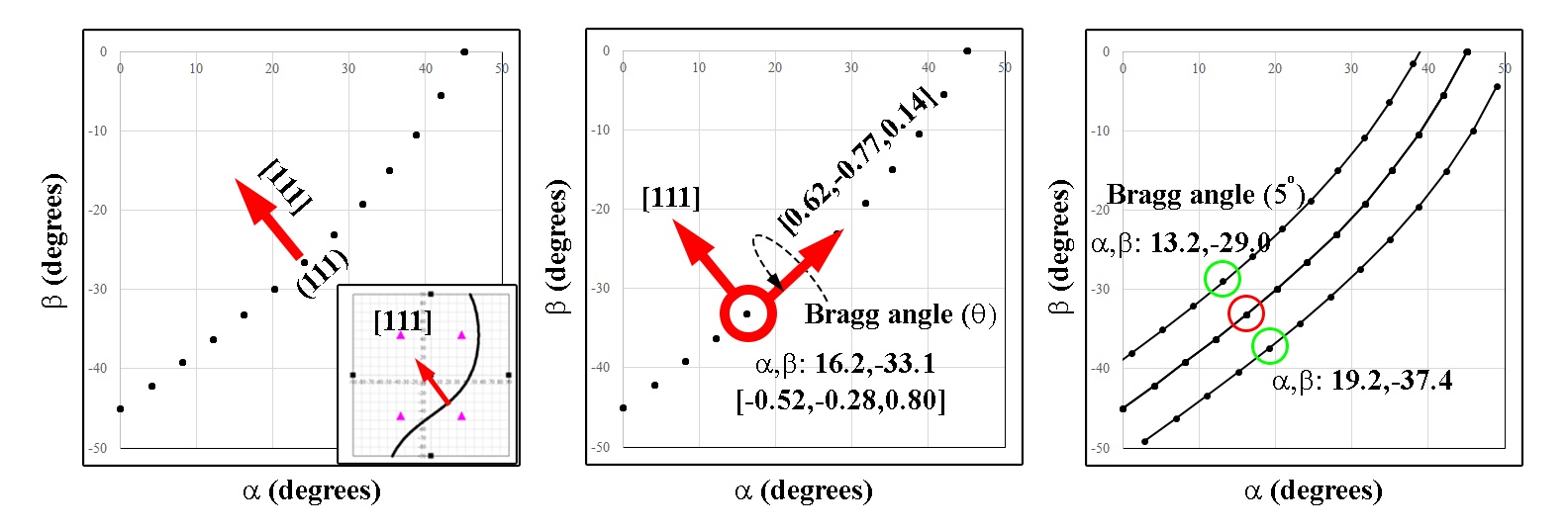
Figure 3.12:Plots of a basic cubic crystal and the trace of the (111) plane, and a Kikuchi bands at a Bragg angle of 5°.
As Kikuchi bands represent dynamical diffraction from crystallographic planes, so too can kinematical diffraction spots also be plotted in a similar fashion, except that instead of plotting lines at the Bragg angle, diffraction spots (±) could be plotted at twice the Bragg angle at any given tilt position within tip/tilt map. The diffraction spots will be dependent upon both the directionality of the plane normal Eq. (2.34) and the structure factor Eq. (2.37) as to whether the plane of atoms is expressed. As demonstrated by Cautaerts et al., if the accuracy of a double tilt stage is sufficient, tilting samples to a two beam condition could be utilized in this manner Cautaerts et al., 2018.
3.11Unknown Crystal Calculator
The development of crystalline stereographic projections, pole figures, and pole figure tip/tilt maps for both general crystals (i.e., for basic low index poles/planes and not derived from the structure factor) in addition to specific crystals (e.g., where the structure factor has filtered specific poles/planes) has been demonstrated to be a powerful tool for studying crystalline materials using a double tilt stage Duden et al., 2009Klinger & Jäger, 2015Li, 2016Liu, 1994Liu, 1995Qing, 1989Qing et al., 1989Xie & Zhang, 2020. Yet, when the crystal structure is unknown, especially for nanocrystalline materials, these calculations are ineffective because the poles/planes discovered can represent any particular crystal and many systems share similar diffraction patterns among various poles/planes. Therefore, it is necessary to develop a methodology to map unknown crystals using the aforementioned protocols, specifically the interface calculator.
Just as the interface calculator was based off the prediction of planes of atoms, so too can the inverse be applied for unknown crystals given the knowledge of what diffraction patterns and Kikuchi bands represent. Diffraction spots (g-vectors) and Kikuchi lines represent the directionality of planes of atoms within a crystal, and therefore can be treated as interfaces. The interface calculator was derived to predict motion of the traces of interfaces, and therefore it can be extended to unknowns. At first, the concept may seem trivial, but when extended to tracing the motion of a single diffraction spot or Kikuchi band in combination with the knowledge that planes of atoms intersect at crystallographic poles, the complexity of the protocol becomes more relevant (Figure 3.13). Regardless of whether the g-vector of a plane is deduced from an atomic column image/fast Fourier transform (Figure 3.13a) or a diffraction pattern (Figure 3.13b), the trace of the plane of atoms can be calculated with relation to the calibrated α tilt axis (given that the plane of atoms is normal to the g-vector) and the tilt conditions at which the g-vector was observed. Similarly, using CBED or Ronchigram mode where a Kikuchi pattern can be collected (Figure 3.13c), the orientation of the trace of the plane at the given tilt conditions can also be plotted.
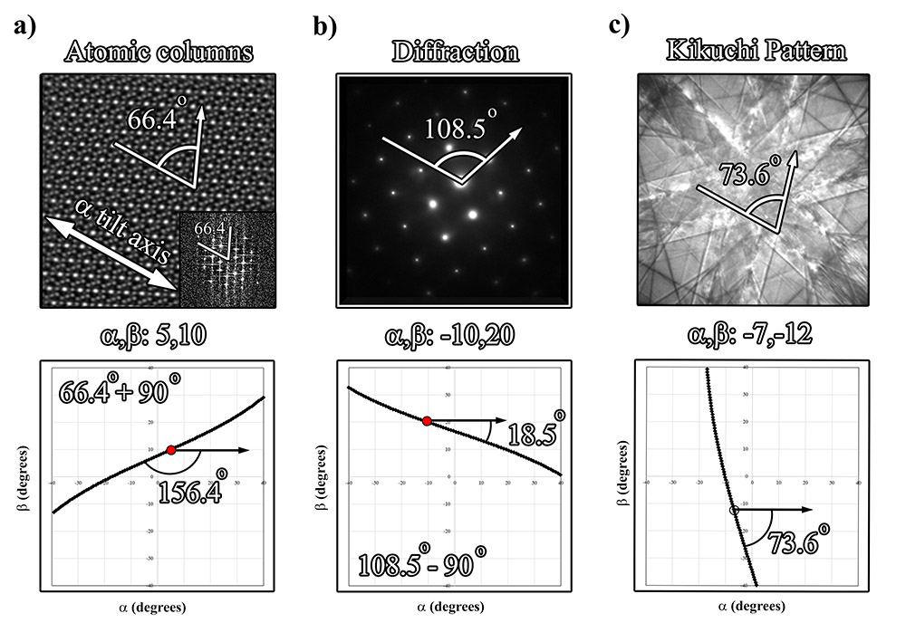
Figure 3.13:Mapping crystallographic planes using (S)TEM images and tilt conditions in a double tilt stage using either a) atomic columns, b) diffraction patterns, c) Kikuchi lines.
This technique can be utilized in a variety of manners to solve for unknowns, from crystals on the order of tens of nanometers to single crystals within a polycrystalline matrix. As a theoretical example, given one g-vector at specific tip/tilt coordinates (red dot, α,β:5,10, with the plane measured at 135° to the α tilt axis), the trace of that plane of atoms within the tilt range of the stage can be calculated (Figure 3.14). This would be similar to tracing a plane of atoms by any of the three means in Figure 3.13. By tilting along that g-vector, additional g-vectors associated with that crystal will eventually come into a diffracting condition (e.g., blue dot, α,β:-19.7,-25.2). Note that as this is a theoretical example, a random point along the line was chosen.
At these new tip/tilt coordinates the directions for any additional planes can be traced, thereby creating a map of that specific crystal (blue dot, Figure 3.14b, 90° at α,β:-19.7,-25.2). Once two poles have been identified and mapped (second pole, green dot, at α,β:-13.3,-23.5), the specific directions for at least one additional pole will be provided through the intersection of the trace of the planes of the individual poles. Without ever having tilted to that position with the stage (third pole, pink spot, α,β:22.9,15.7), the knowledge that there is a pole present provides assurance to the microscopist that additional poles can be quickly determined. As illustrated in Figure 3.14b, the weight of each trace can be scaled according to the apparent indexing of the planes (i.e., low index planes will appear darker due to multiple planes expressed due to the structure factor). This can further be used as a fingerprinting technique for analyzing unknowns. To illustrate how this would work in practice, a movie highlighting the identification of an austenitic stainless steel grain is shown in Figure 3.14c.
Lastly, once a number of poles have been identified and planes traced, additional crystallographic information can be garnered from the map. For example, the pure tilt angles between poles can be calculated Eq. (3.14), poles not attainable in the tilt stage will be apparent, and finally symmetry of the system can be observed and tested. If a mirror plane is suspected, tilting to specific angles to either side of the plane can be performed to observe whether identical diffraction patterns are exhibited. The collection of this data can then be used to identify a large number of poles within a sample to compare to crystallographic mapping programs such as Crystal Maker Palmer, 2015 or JEMS Stadelmann, 1987.
- Carter, B., Carter, D., & Williams, D. (1996). Transmission Electron Microscopy: A Textbook for Materials Science. Diffraction. II. Springer. https://doi.org/10.1007/978-0-387-76501-3
- Kondo, Y., Ito, T., & Harada, Y. (1984). New Electron Diffraction Techniques Using Electronic Hollow-Cone Illumination. Japanese Journal of Applied Physics, 23, L178–L180. https://doi.org/10.1143/JJAP.23.L178
- Vincent, R., & Midgley, P. A. (1994). Double conical beam-rocking system for measurement of integrated electron diffraction intensities. Ultramicroscopy, 53, 271–282. https://doi.org/10.1016/0304-3991(94)90039-6
- Midgley, P., & Eggeman, A. (2015). Precession electron diffraction - A topical review. IUCrJ, 2(2), 126–136. https://doi.org/10.1107/S2052252514022283
- Spurgeon, S. R., Ophus, C., Jones, L., Petford-Long, A., Kalinin, S. V., Olszta, M. J., Dunin-Borkowski, R. E., Salmon, N., Hattar, K., Yang, W.-C. D., Sharma, R., Du, Y., Chiaramonti, A., Zheng, H., Buck, E. C., Kovarik, L., Penn, R. L., Li, D., Zhang, X., … Taheri, M. L. (2020). Towards data-driven next-generation transmission electron microscopy. Nature Materials. https://doi.org/10.1038/s41563-020-00833-z
- Olszta, M., Hopkins, D., Fiedler, K. R., Oostrom, M., Akers, S., & Spurgeon, S. R. (2022). An Automated Scanning Transmission Electron Microscope Guided by Sparse Data Analytics. Microscopy and Microanalysis, 28(5), 1611–1621. 10.1017/S1431927622012065
- Chesser, I., Francis, T., De Graef, M., & Holm, E. A. (2020). Learning the grain boundary manifold: tools for visualizing and fitting grain boundary properties. Acta Materialia. https://doi.org/10.1016/j.actamat.2020.05.024
- Jeong, H., Seo, S., Hong, H., & Yoo, Y. (2010). Characterization of the parameters relating adjacent grains using transmission electron microscopy. Journal of Applied Crystallography, 43(6), 1495–1501. https://doi.org/10.1107/S002188981004149X
- Liu, Q. (1994). A simple method for determining orientation and misorientation of the cubic crystal specimen. Journal of Applied Crystallography, 27(4), 755–761. https://doi.org/10.1107/S0021889894002062
- Liu, Q. (1995). A simple and rapid method for determining orientations and misorientations of crystalline specimens in TEM. Ultramicroscopy, 60(1), 81–89. https://doi.org/10.1016/0304-3991(95)00049-7
- Blavette, D., Deconihout, B., Bostel, A., Sarrau, J., Bouet, M., & Menand, A. (1993). The tomographic atom probe: A quantitative three-dimensional nanoanalytical instrument on an atomic scale. Review of Scientific Instruments, 64, 2911–2919. https://doi.org/10.1063/1.1144382
- Simonen, E. P., & Bruemmer, S. M. (1998). Radiation effects on environmental cracking of stainless steels. JOM, 50, 52–55. https://doi.org/10.1007/s11837-998-0309-3
- Hayashida, M., Cui, K., Homeniuk, D., Phengchat, R., Blackburn, A., & Malac, M. (2019). Parameters affecting the accuracy of nanoparticle shape and size measurement in 3D. Micron, 123, 102680. https://doi.org/10.1016/j.micron.2019.102680
- Hayashida, M., & Malac, M. (2016). Practical electron tomography guide: Recent progress and future opportunities. Micron, 91, 49–74. https://doi.org/10.1016/j.micron.2016.09.010
- Lidke, D. S., & Lidke, K. A. (2012). Advances in high-resolution imaging–techniques for three-dimensional imaging of cellular structures. Journal of Cell Science, 125, 2571. https://doi.org/10.1242/jcs.090027

